
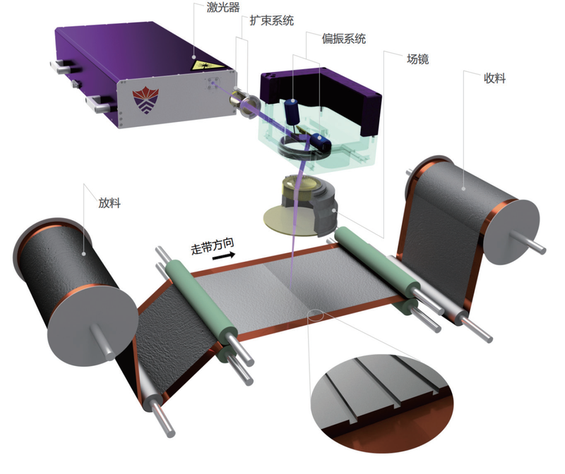
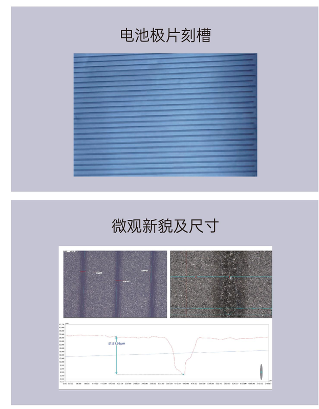
Electrode sheet grooving
The precision laser grooving and drilling system provides high-precision, noncontact micromachining across industries. It creates clean grooves or holes in lithium-battery electrodes to improve performance and safety, and micron-scale ITO-film grooves on optoelectronic materials such as perovskites for precise circuits. It also stresslessly drills or scribes plastic films and forms precision structures on spectral silicon wafers. On hard, brittle materials such as glass and ceramics, it produces grooves with clean edges and no microcracks. Consumable-free, pollution-free processing supports flexible production in new energy, optoelectronic displays and precision components.
 Save to Favorites
Overview
Specifications
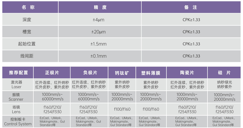
| Parameter | Value |
|---|---|
| Depth Accuracy [CPK≥1.33] | ±4μm |
| Slot width Accuracy [CPK≥1.33] | ±20μm |
| Starting position accuracy [CPK≥1.33] | ±1.5mm |
| Line spacing accuracy [CPK≥1.33] | ±0.1mm |
Applications
Key Features
Datasheet
Please provide your email to download the datasheet.
Invalid email format. Please try again.
Supplier Information
Related Products
-
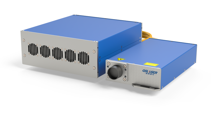 100W Subnanosecond Infrared Laser
Laser Modules & Systems
Guoshunlaser
M² Beam quality: <1.6 Average Output Power: >100 Power adjustment Range: 0~100 %
-
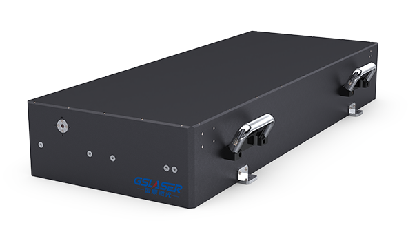 100W Picosecond Green Fiber Laser
Laser Modules & Systems
Guoshunlaser
M² Beam quality: <1.3 Average Output Power: >100 Power adjustment Range: 0~100 %
-
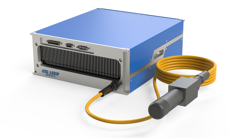 100W Nanosecond Infrared Fiber Laser
Laser Modules & Systems
Guoshunlaser
M² Beam quality: <1.4 Average Output Power: >100 Power adjustment Range: 0~100 %
-
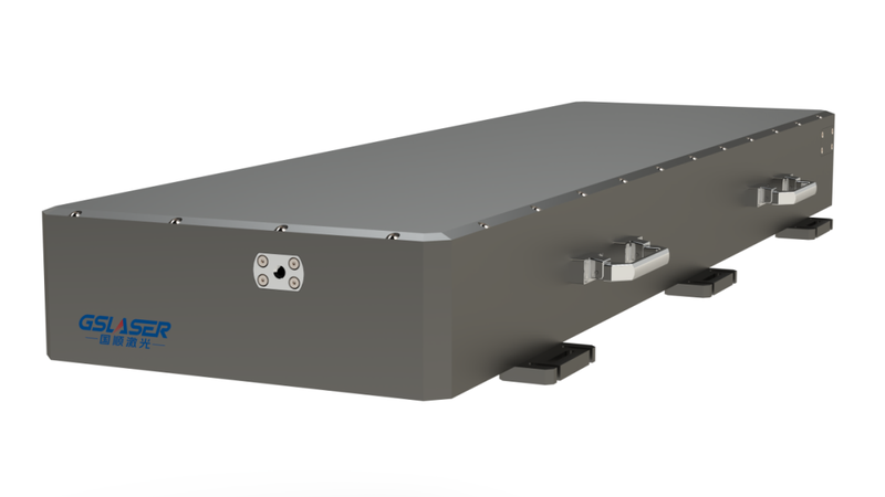 100W Femtosecond Infrared Laser
Laser Modules & Systems
Guoshunlaser
M² Beam quality: <1.3 Average Output Power: >100 Power adjustment Range: 0~100 %
-
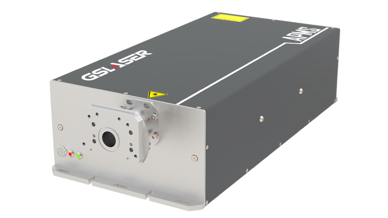 10W Compact Picosecond Infrared Laser
Laser Modules & Systems
Guoshunlaser
M² Beam quality: <1.2 Average Output Power: >10 Power adjustment Range: 0~100 %
Related Articles
As a core precision optical component for wavelength screening, frequency locking and spectral demodulation, optical etalons are widely used in high-end scientific research and precision laser equipment.
As a vital emerging sector of modern three-dimensional spatial economy, the low-altitude economy has become a new global growth driver. It covers a wide range of commercial scenarios, including UAV navigation and obstacle avoidance, precise airspace management, aerial mapping, low-altitude logistics distribution, security monitoring and emergency disaster rescue. Nevertheless, frequent extreme weather, complex terrain obstacles and increasingly dense low-altitude flight activities pose severe challenges to the safety and stability of low-altitude aircraft operations.
Laser pump sources are the core energy input component of solid-state lasers and laser amplifiers, and their performance directly determines the output power, beam quality and service life of the entire laser system. In scenarios such as industrial processing, scientific research experiments and high-end equipment, improper pump source selection will not only result in substandard system performance, but also bring a series of problems such as rapid device degradation and high operation and maintenance costs. This article sorts out the core selection logic and key pitfalls of pump source procurement, and provides selection references based on mature, mass-produced high-reliability products to help purchasers efficiently screen suitable products.
Shandong Haucore Optoelectronics Co., Ltd. introduces the HGLD‑792‑COS‑D‑10WB semiconductor laser within its COS series. Delivering an output power of 10 W at a central wavelength of 792 nm, this device adopts gold‑tin bonding COS packaging. Featuring high reliability and long service life, it serves as a preferred pump source for solid‑state lasers and is widely deployed in industrial processing, laser display, medical & aesthetic treatment, scientific research and other fields.
Loading...
Name
Phone
Organization
Use Case

Database Platform