
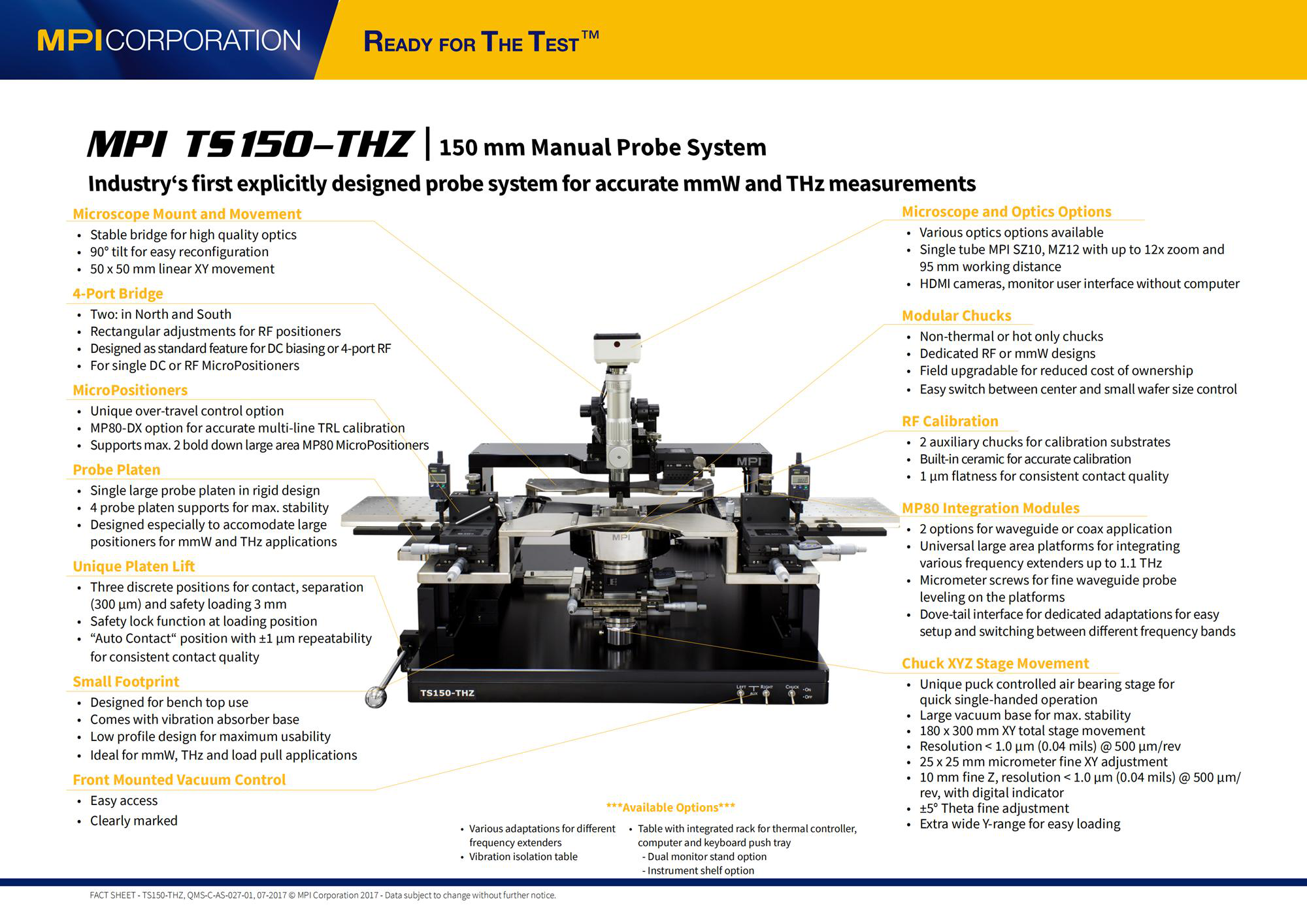


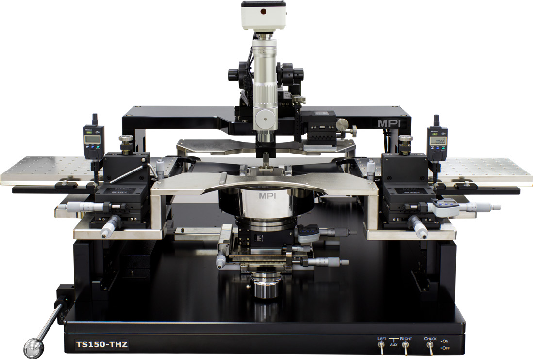

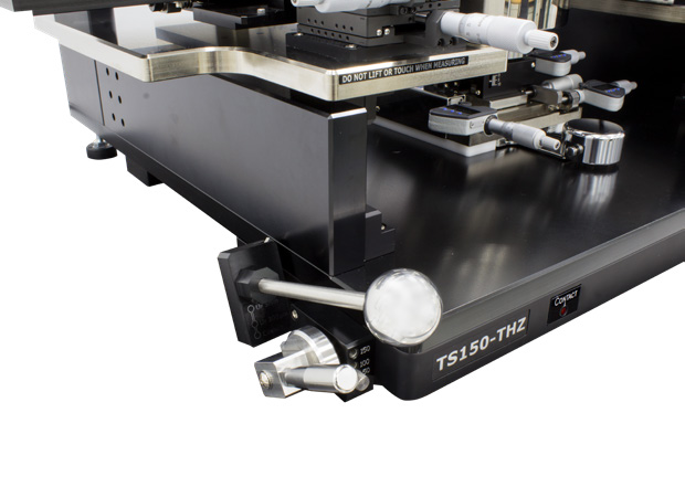
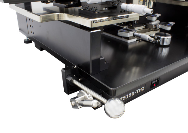
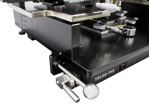

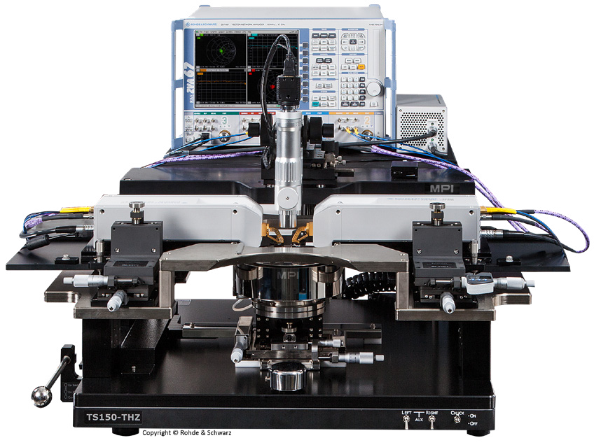

MPI TS150-THZ 150 mm Manual Probe System
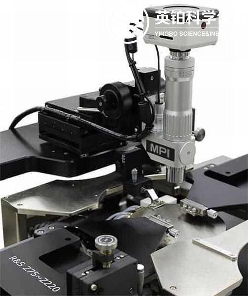
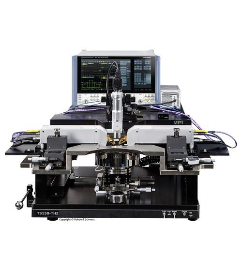
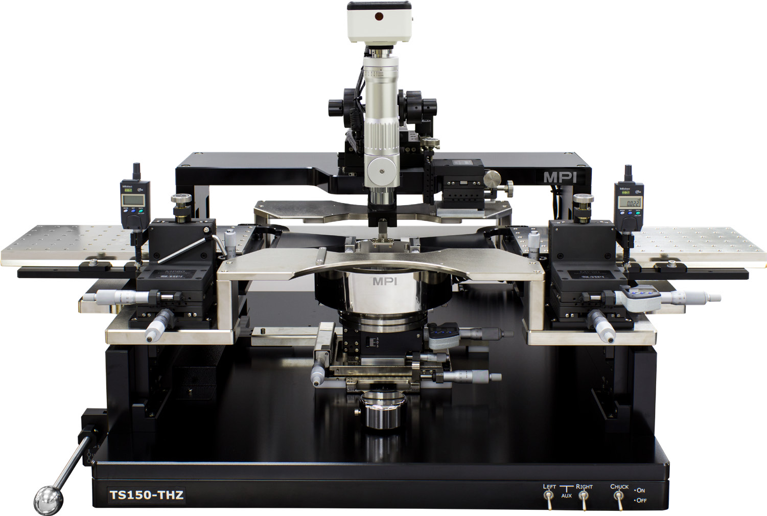
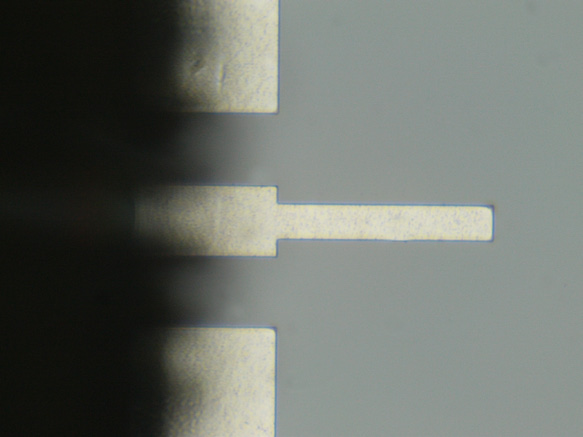
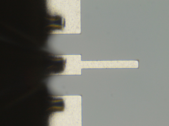
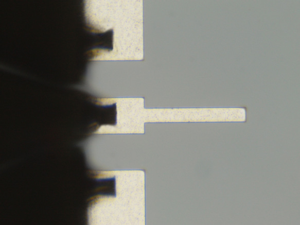
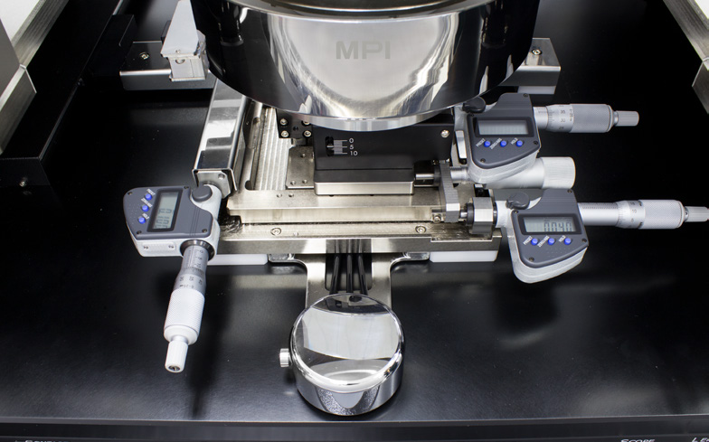
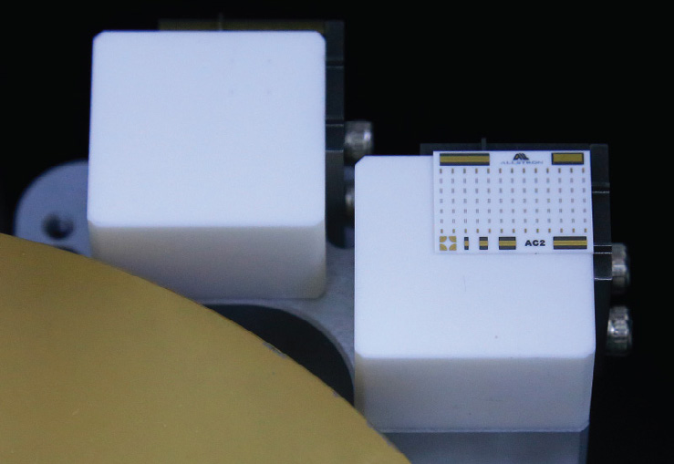
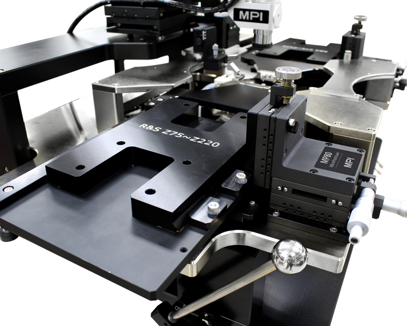
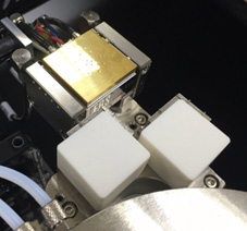
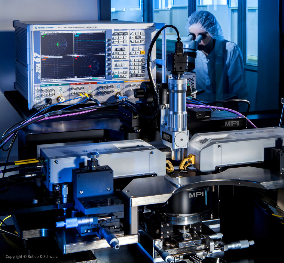
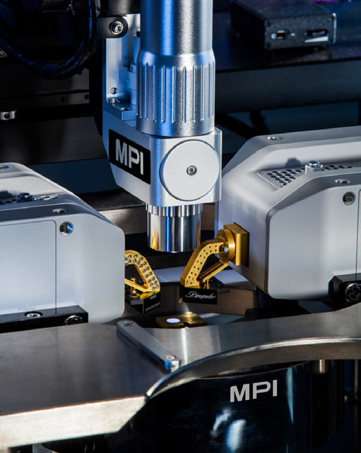
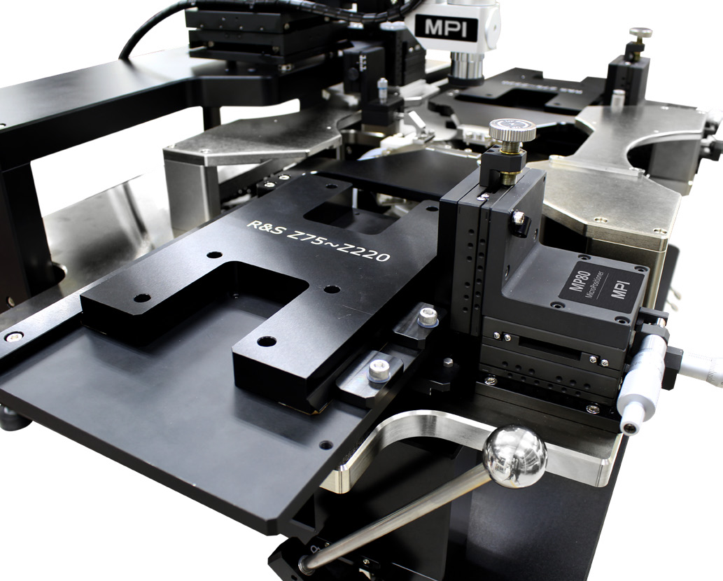
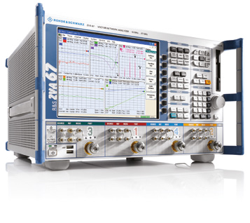
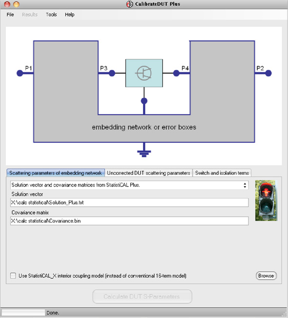
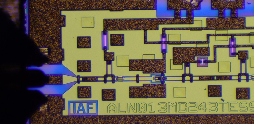
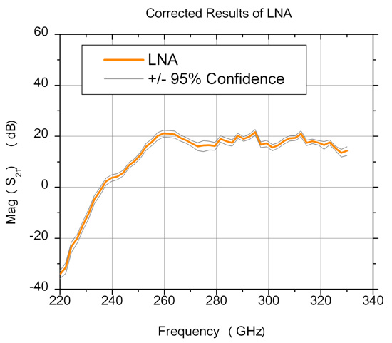
The MPI TS150-THZ is a manual probe system explicitly designed for accurate mmW and THz measurements, offering seamless integration with VNA frequency extenders and advanced calibration techniques.
 Save to Favorites
Overview
Specifications
| Parameter | Value |
|---|---|
| Total Travel Range | 180x300mm (7.1x11.8in) |
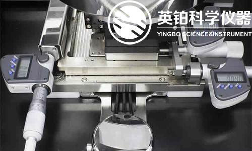
| Fine-travel range | 25x25mm |
| Fine-travel resolution | <1.0μm (0.04mils)@500μm/rev |
| Planarity | <10μm |
| Theta Travel (Standard) | 360° |
| Theta Travel (Fine) | ±5.0° |
| Theta Resolution | 7.5x10^-3 gradient |
| Travel Range | 10mm (0.4in) |
| Movement Range | 50x50mm (2x2in) |
| Resolution | <5μm (0.2mils) |
| Probe Platen Design | Nickel plated steel |
| Probe Platen Design | low profile |
| Probe Platen Design | four pole support |
| Platen Lift Control | 3 positions - contact (0), separation (300μm), loading (3mm) |
| Separation Repeatability | <1μm (0.04mils) |
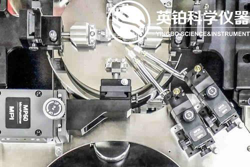
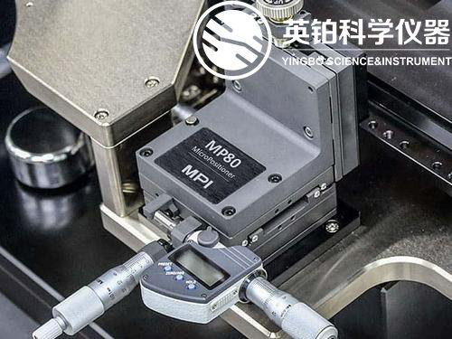
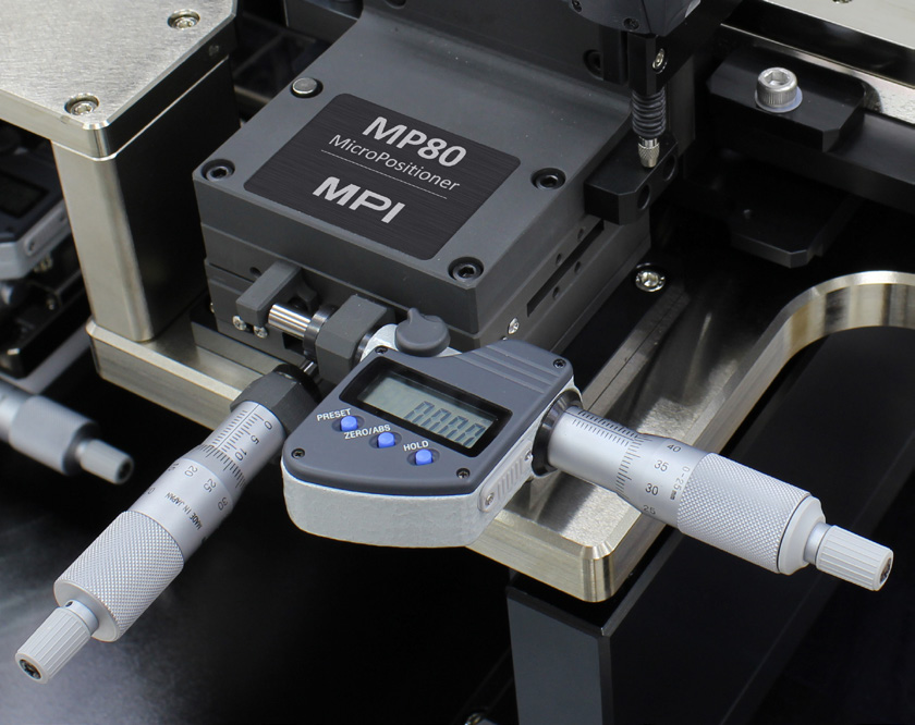
| RF MicroPositioner Mounting | Magnetic with guided rail |
| DC MicroPositioner Mounting | Magnetic |
| RF Wafer Chuck Diameter | 160mm |
| RF Wafer Chuck Material | Nickel plated aluminum |
| Surface Planarity | ≤5μm |
| Rigidity | <15μm/10N@edge |
| mmW Wafer Chuck Diameter | 160mm |
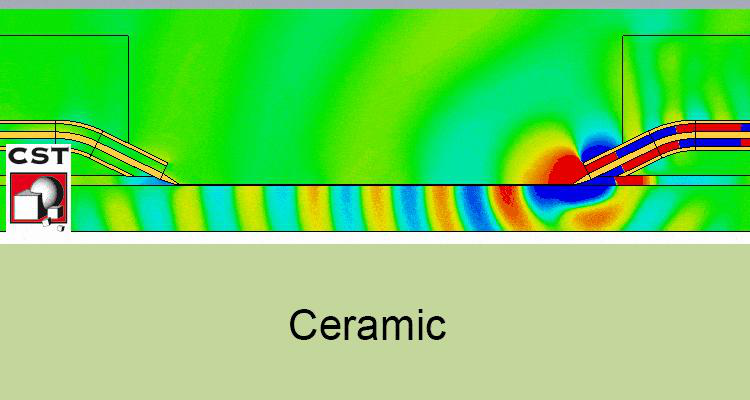
| mmW Wafer Chuck Material | Ceramic |
| Maximal wafer size | 150mm |
| Temperature Control Method | Cooling air/Resistance heater |
| Coolant | Air (user supplied) |
| Temperature Stability | ±0.5°C |
| Temperature Accuracy | ±1°C |
| Surface Flatness | <15μm |
| Electrical Isolation | >0.5TΩ@25°C |
| Capacitance | <750pF |
| Maximum Voltage Between Chuck Top and GND | 500V DC |
| Vibration Isolation Table Dimensions (Standard) | 900x800x835mm (35.4x31.5x32.9in) |
| Vibration Isolation Table Dimensions (Advanced) | 900x800x830mm (35.4x31.5x32.7in) |
| Weight | Approx. 210kg (463lb) |
Applications
Key Features
Datasheet
Supplier Information
Related Products
-
 futureD Semiconductor Big Data System
Probe Station
Eoulu
futureD Semiconductor Big Data System
Probe Station
Eoulu
Server Room: 不同断电源、温度、湿度适宜,防尘 Operating System: win10; 64位操作系统 Processor: 6核
futureD is a big data processing tool designed to help customers process massive data generated during semiconductor testing. It simplifies calculations, making data processing faster and more efficient.
-
 SWIT-009
Probe Station
Eoulu
SWIT-009
Probe Station
Eoulu
Number of Input Ports: 12 Number of Output Ports: 18 Maximum Operating Voltage: 3000V
SWIT-009 is a high-performance matrix switch designed for precise and efficient signal routing in various applications. It features advanced technical specifications and robust design, making it suitable for demanding environments.
-
 TS150 Manual Probe System
Probe Station
Ybsemi-Solution
TS150 Manual Probe System
Probe Station
Ybsemi-Solution
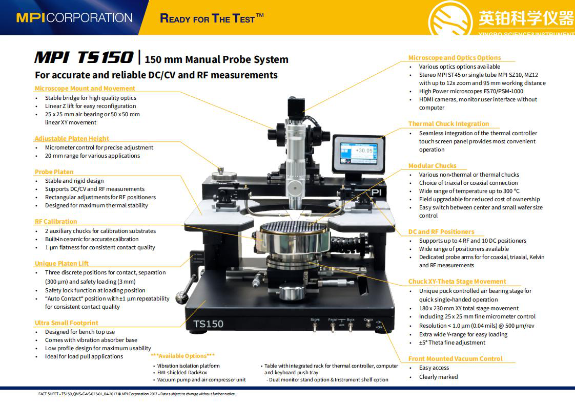
Total Travel Range: 180x230mm (7.1x9.1in) Fine Travel Range: 25x25mm fine micrometer control Fine Travel Resolution: <1.0μm (0.04mils)@500μm/rev
The TS150 is a 150 mm manual probe system designed for accurate and reliable DC/CV and RF measurements, offering high precision and flexibility for various applications.
-
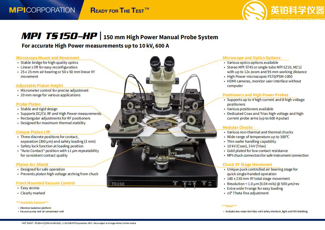 MPI TS200-HP
Probe Station
Ybsemi-Solution
MPI TS200-HP
Probe Station
Ybsemi-Solution
Probe Station Dimensions: 900×1050×1930mm Weight: ~500kg Chuck XY Stage Travel Range: 225×260mm
The MPI TS200-HP is a 200 mm manual probe system designed for accurate and reliable high-power measurements up to 10 kV and 600 A. It features advanced EMI/RFI shielding, ergonomic design, and compatibility with various accessories for high voltage and high current applications.
-
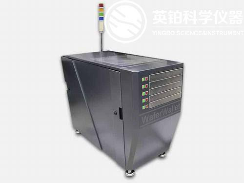 TS3500-SE
Probe Station
Ybsemi-Solution
TS3500-SE
Probe Station
Ybsemi-Solution
Chuck XY Stage Travel Range: 310mm×530mm Resolution: 0.0001° (0.24μm @ 300mm edge) Accuracy: <2.0μm
The TS3500-SE is a 300 mm automated probe system designed for accurate and reliable IV, CV, pulsed-IV, 1/f, and RF measurements. It features advanced EMI shielding, ultra-low noise IV measurements, and programmable microscope movements for test automation.
Related Articles
Electro-optic deflectors (EODs) are optical devices used to steer or deflect light beams by applying an electric field to a specialized optical crystal. Unlike mechanical beam steering systems that rely on moving mirrors, electro-optic deflectors enable high-speed, non-mechanical beam control with exceptional precision and responsiveness. They are widely used in laser scanning, optical communications, microscopy, laser printing, spectroscopy, and scientific research, where rapid and accurate laser beam positioning is essential.
An infrared transmitter (IR transmitter) is a basic electronic component that sends invisible infrared light signals for short-range wireless control. It is widely used in daily electronics, smart home devices, and industrial equipment due to its low cost, low power consumption, and stable performance.
Shanghai Connet Laser Technology Co., Ltd. focuses on technological innovation, delivering cutting-edge photonic products & solutions for industrial lasers, LiDAR, fiber optic sensing, coherent telecom, cold atom physics and precision spectroscopy research & mass manufacturing.
Wuhan Optical Valley Interlink Technology Co., Ltd. was founded in 2013 by a technical team from Huazhong University of Science and Technology.
Loading...
Name
Phone
Organization
Use Case

Database Platform