
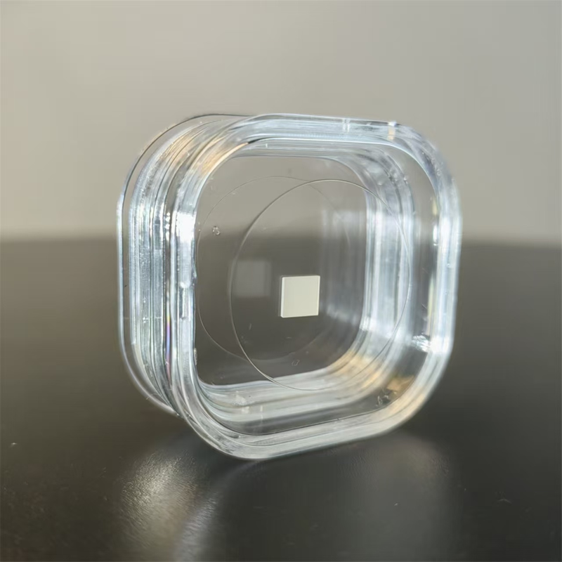
Strontium Titanate STO
SrTiO₃ STO Perovskite Single-Crystal Substrate,Good Lattice Match/High Dielectric Constant/Transparency/Chemical Stability,for High-Tc Superconductors,Ferroelectric,Optoelectronic/Microelectronics.
 Save to Favorites
Overview
Specifications
| Parameter | Value |
|---|---|
| STO Strontium Titanate Substrate - Dimensions | 5 mm × 5 mm |
| STO Strontium Titanate Substrate - Dimensions | 10 mm × 10 mm |
| STO Strontium Titanate Substrate - Thickness | 0.5mm |
| STO Strontium Titanate Substrate - Main Surface Crystal Orientation | <100>、<001>、<111> |
| STO Strontium Titanate Substrate - Surface Condition | Single-Side Polished SSP, Double-Side Polished DSP |
| STO Strontium Titanate Substrate - Doping | Undoped, Nb-Doped, Fe-Doped |
| STO Strontium Titanate Substrate - Roughness | <0.2nm |
| Crystal Configuration | Perovskite ABO₃, Cubic Phase (Room Temperature) |
| Lattice Constant | 3.905 Å |
| Melting Point | 2080 ℃ |
| Mohs Hardness | 6.0~6.5 |
| Room-Temperature Permittivity [1MHz] | ≈300(1MHz) |
| Intrinsic Resistivity | 10¹²~10¹⁴ Ω·cm |
| Bandgap | 3.2 eV |
| Transmission Interval | 0.38~5 μm (UV-Mid-Infrared) |
| Visible-Light Refractive Index | 2.4 |
| Chemical Stability | Acid/Alkali Resistant, Oxidation Resistant, No Solid-Phase Diffusion |
Applications
Key Features
Datasheet
Please provide your email to download the datasheet.
Invalid email format. Please try again.
Supplier Information
Related Products
-
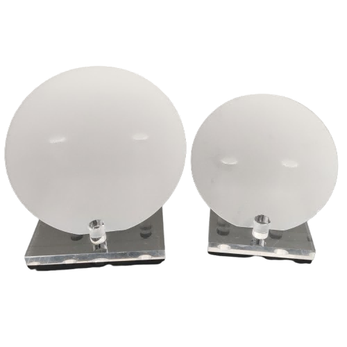 Sapphire A-R-M Special Crystal-Orientation Substrate
Optical Material
Jmwafer
A-M-R Orientation Single-Crystal Sapphire Substrate (2~6 Inches) - Material Composition: >99.99%,High Purity, Mono-crystalline Al2O3 (KY) Sapphire A/M/R-Plane Single-Crystal Substrate (2~6 Inches) - End-Face Crystal Orientation [Diameter: 50.8mm]: A-plane (11-20) ± 0.1° Sapphire A/M/R-Plane Single-Crystal Substrate (2~6 Inches) - End-Face Crystal Orientation [Diameter: 100mm]: A-plane (11-20) ± 0.1°
α-Al2O3 Hexagonal Lattice,Chemically Stable/Water-Insoluble/Strong Acid-Alkali Resistant,Mohs9,Melts2050℃/Boils3500℃,Operating up to1900℃,Good Transmission/Thermal Conduction/Insulation/Mechanics,Wear/Scratch Resistance.
-
 N-Type Silicon Carbide Epitaxy
Optical Material
Jmwafer
N-Type Silicon Carbide Epitaxial Substrate (2~8 Inches) - Substrate Diameter: 2 inch - 50.8mm N-Type Silicon Carbide Epitaxial Substrate (2~8 Inches) - Substrate Diameter: 4 inch - 100mm N-Type Silicon Carbide Epitaxial Substrate (2~8 Inches) - Substrate Diameter: 6 inch - 150mm
N-Type SiC Epitaxy Grows N-Doped Layer on SiC,High Electron Mobility/Thermal Conductivity/Breakdown Field.
-
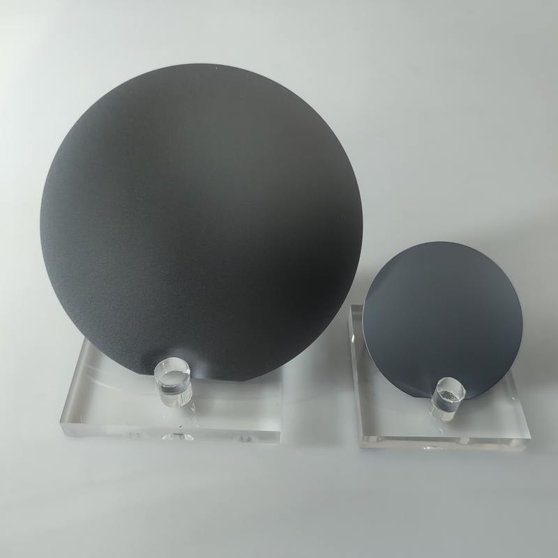 Silicon-Based GaN Epitaxial Template
Optical Material
Jmwafer
Silicon-Based GaN Epitaxial Template Substrate (2~8 Inches) - Substrate Diameter: 50.8mm Silicon-Based GaN Epitaxial Template Substrate (2~8 Inches) - Substrate Diameter: 100mm Silicon-Based GaN Epitaxial Template Substrate (2~8 Inches) - Substrate Diameter: 150mm
GaN-on-Si Epitaxy Grows GaN Films on Silicon,Combining GaN Performance with Low-Cost Silicon.
-
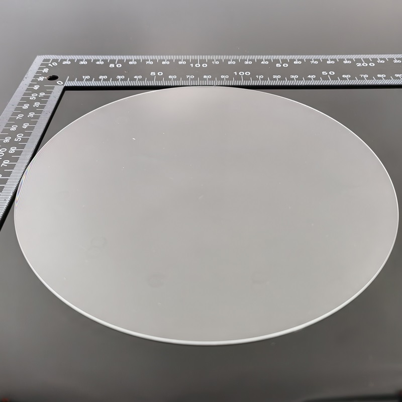 High-Borosilicate Glass BF33
Optical Material
Jmwafer
High-Borosilicate Glass - Material: BF33 High-Borosilicate Glass - Diameter: 50.8mm High-Borosilicate Glass - Diameter: 100mm
BF33 Special Borosilicate Glass with Low Expansion,Heat Resistance,Chemical Stability and Excellent Transmission.
-
 Sapphire-Based GaN Epitaxial Template
Optical Material
Jmwafer
Sapphire-Based GaN Epitaxial Template Substrate (2~8 Inches) - Substrate Diameter: 50.8mm Sapphire-Based GaN Epitaxial Template Substrate (2~8 Inches) - Substrate Diameter: 100mm Sapphire-Based GaN Epitaxial Template Substrate (2~8 Inches) - Substrate Diameter: 150mm
GaN-on-Sapphire Epitaxial Template Grows GaN Film on Al₂O₃,Common Substrate for Heat/Chemical Stability/Cost Advantages.
Related Articles
Raybowlaser, a professional manufacturer of high-power laser chips, has officially launched its upgraded new-generation 1470nm high-performance laser chip. Achieving groundbreaking progress in rated output power and wall-plug efficiency (WPE), this innovative laser chip delivers superior and reliable core light source solutions for medical cosmetology, industrial processing, agricultural applications and scientific research equipment.
Electro-optic deflectors (EODs) are optical devices used to steer or deflect light beams by applying an electric field to a specialized optical crystal. Unlike mechanical beam steering systems that rely on moving mirrors, electro-optic deflectors enable high-speed, non-mechanical beam control with exceptional precision and responsiveness. They are widely used in laser scanning, optical communications, microscopy, laser printing, spectroscopy, and scientific research, where rapid and accurate laser beam positioning is essential.
Founded in 2004, Wuhan Union Optic Inc. is a National Specialized, Refined, Unique & Innovative "Little Giant" high-tech enterprise located in Wuhan East Lake High-Tech Development Zone.
Precise spectral screening is essential for high-precision medical detection, spectroscopic analysis and intelligent imaging systems. Tailored for visible and near-infrared spectral separation, the SP900 shortpass optical filter delivers high-efficiency light transmission and deep infrared blocking performance. It effectively eliminates stray light interference, improves signal-to-noise ratio (SNR), and serves as a core optical component for biomedical instruments, scientific analysis equipment and machine vision systems.
Loading...
Name
Phone
Organization
Use Case

Database Platform