
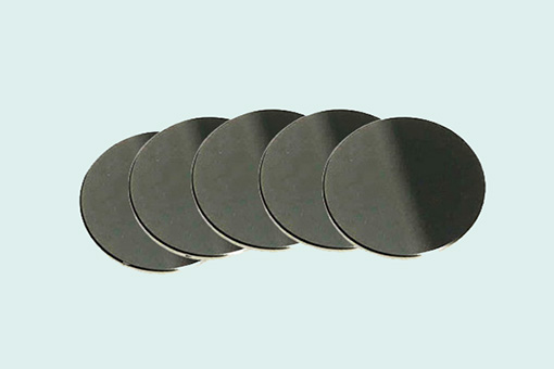
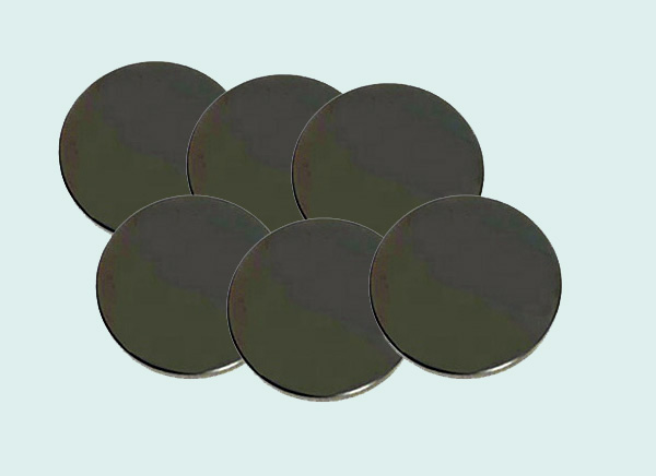
Si Windows
Silicon is a mono crystal primarily used in semi-conductor and is non-absorptive at 1.2μm to 6μm IR regions. It is used here as an optical component for IR region applications. Silicon is used as an optical window primarily in the 3 to 5 micron band and as a substrate for production of optical filters. Large blocks of Silicon with polished faces are also employed as neutron targets in Physics experiments. Silicon is grown by Czochralski pulling techniques (CZ) and contains some oxygen which causes an absorption band at 9 microns. To avoid this, Silicon can be prepared by a Float-Zone (FZ) process. Optical Silicon is generally lightly doped ( 5 to 40 ohm cm) for best transmission above 10 microns. Silicon has a further pass band 30 to 100 microns which is effective only in very high resistivity uncompensated material. Doping is usually Boron (p-type) and Phosphorus (n-type). Material: Si Diameter Tolerance: +0.0/-0.1mm Thickness Tolerance: ±0.1mm Surface Accuracy: λ/4@632.8nm Parallelism: <1' Surface Quality: 60-40 Clear Aperture: >90% Bevelling: <0.2×45° Coating: Custom Design
 Save to Favorites
Overview
Specifications
| Parameter | Value |
|---|---|
| Transmission Range | 1.2 to 15 μm |
| Refractive Index [5 μm] | 3.4223 @ 5 μm |
| Reflection Loss [5 μm;2 surfaces] | 46.2% at 5 μm (2 surfaces) |
| Absorption Coefficient [3 μm] | 0.01 cm⁻¹ at 3 μm |
| dn/dT | 160 x 10⁻⁶ /°C |
| dn/dμ = 0 | 10.4 μm |
| Density | 2.33 g/cc |
| Melting Point | 1420 °C |
| Thermal Conductivity [273 K] | 163.3 W m⁻¹ K⁻¹ at 273 K |
| Thermal Expansion [20°C] | 2.6 x 10⁻⁶ / at 20°C |
| Hardness | Knoop 1150 |
| Specific Heat Capacity | 703 J Kg⁻¹ K⁻¹ |
| Dielectric Constant [10 GHz] | 13 at 10 GHz |
| Youngs Modulus (E) | 131 GPa |
| Shear Modulus (G) | 79.9 GPa |
| Bulk Modulus (K) | 102 GPa |
| Elastic Coefficients | C₁₁=167; C₁₂=65; C₄₄=80 |
| Apparent Elastic Limit | 124.1MPa (18000 psi) |
| Poisson Ratio | 0.266 |
| Solubility | Insoluble in Water |
| Molecular Weight | 28.09 |
| Class/Structure | Cubic diamond, Fd3m |
Applications
Key Features
Datasheet
Supplier Information
Related Products
-
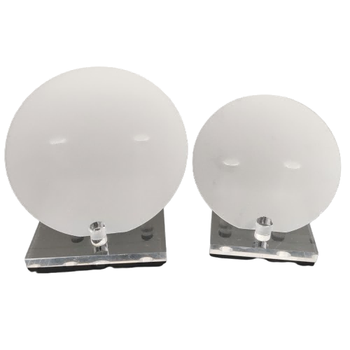 Sapphire A-R-M Special Crystal-Orientation Substrate
Optical Material
Jmwafer
A-M-R Orientation Single-Crystal Sapphire Substrate (2~6 Inches) - Material Composition: >99.99%,High Purity, Mono-crystalline Al2O3 (KY) Sapphire A/M/R-Plane Single-Crystal Substrate (2~6 Inches) - End-Face Crystal Orientation [Diameter: 50.8mm]: A-plane (11-20) ± 0.1° Sapphire A/M/R-Plane Single-Crystal Substrate (2~6 Inches) - End-Face Crystal Orientation [Diameter: 100mm]: A-plane (11-20) ± 0.1°
α-Al2O3 Hexagonal Lattice,Chemically Stable/Water-Insoluble/Strong Acid-Alkali Resistant,Mohs9,Melts2050℃/Boils3500℃,Operating up to1900℃,Good Transmission/Thermal Conduction/Insulation/Mechanics,Wear/Scratch Resistance.
-
 N-Type Silicon Carbide Epitaxy
Optical Material
Jmwafer
N-Type Silicon Carbide Epitaxial Substrate (2~8 Inches) - Substrate Diameter: 2 inch - 50.8mm N-Type Silicon Carbide Epitaxial Substrate (2~8 Inches) - Substrate Diameter: 4 inch - 100mm N-Type Silicon Carbide Epitaxial Substrate (2~8 Inches) - Substrate Diameter: 6 inch - 150mm
N-Type SiC Epitaxy Grows N-Doped Layer on SiC,High Electron Mobility/Thermal Conductivity/Breakdown Field.
-
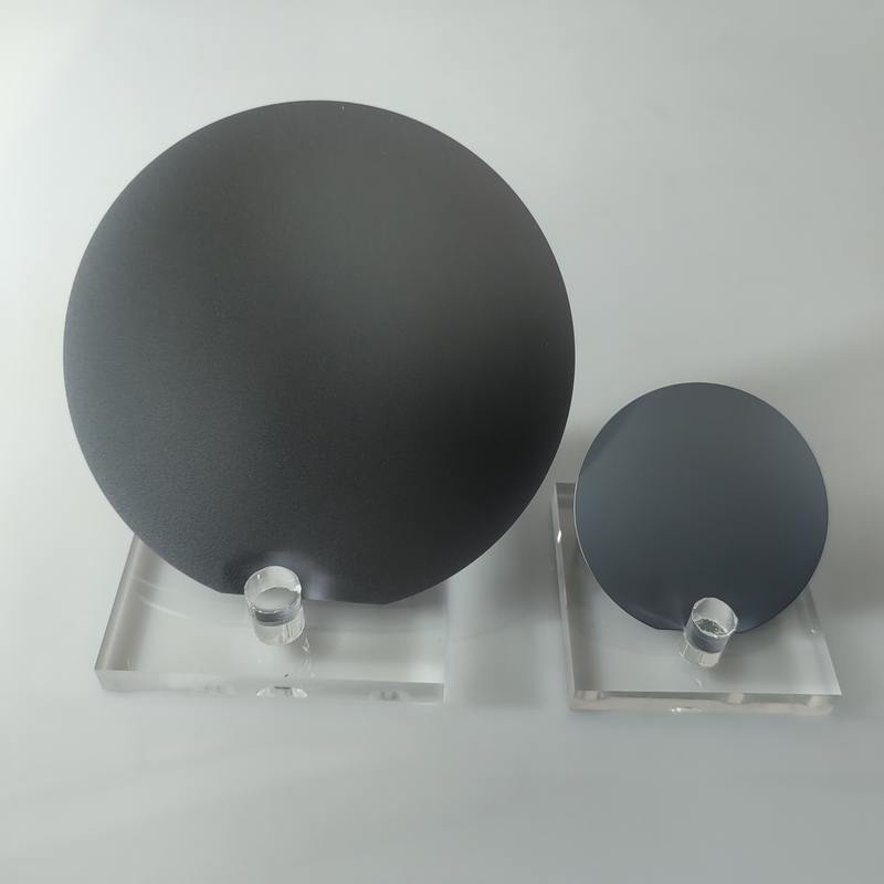 Silicon-Based GaN Epitaxial Template
Optical Material
Jmwafer
Silicon-Based GaN Epitaxial Template Substrate (2~8 Inches) - Substrate Diameter: 50.8mm Silicon-Based GaN Epitaxial Template Substrate (2~8 Inches) - Substrate Diameter: 100mm Silicon-Based GaN Epitaxial Template Substrate (2~8 Inches) - Substrate Diameter: 150mm
GaN-on-Si Epitaxy Grows GaN Films on Silicon,Combining GaN Performance with Low-Cost Silicon.
-
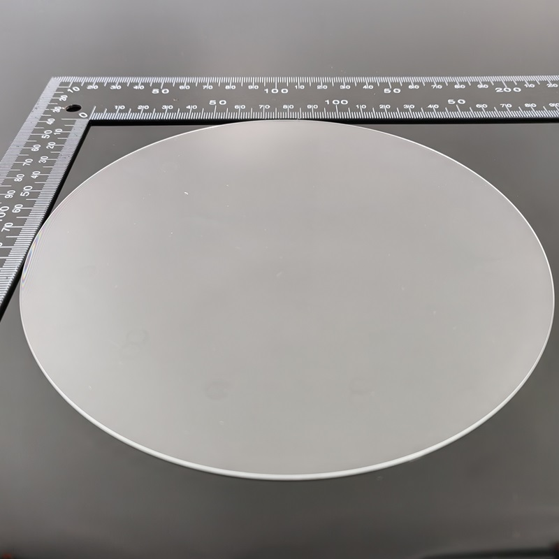 High-Borosilicate Glass BF33
Optical Material
Jmwafer
High-Borosilicate Glass - Material: BF33 High-Borosilicate Glass - Diameter: 50.8mm High-Borosilicate Glass - Diameter: 100mm
BF33 Special Borosilicate Glass with Low Expansion,Heat Resistance,Chemical Stability and Excellent Transmission.
-
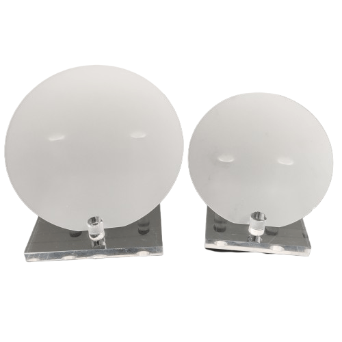 Sapphire-Based GaN Epitaxial Template
Optical Material
Jmwafer
Sapphire-Based GaN Epitaxial Template Substrate (2~8 Inches) - Substrate Diameter: 50.8mm Sapphire-Based GaN Epitaxial Template Substrate (2~8 Inches) - Substrate Diameter: 100mm Sapphire-Based GaN Epitaxial Template Substrate (2~8 Inches) - Substrate Diameter: 150mm
GaN-on-Sapphire Epitaxial Template Grows GaN Film on Al₂O₃,Common Substrate for Heat/Chemical Stability/Cost Advantages.
Related Articles
The accelerated construction of new‑generation power systems has brought revolutionary upgrades to power‑equipment maintenance workflows.
Driven by fast‑growing demands of 3D perception, biometric authentication and machine‑vision industries, near‑infrared imaging optics have become a vital hardware component for intelligent sensing systems.
icrolight is a high-tech enterprise specializing in the R&D, manufacturing and sales of active and passive photonic devices for microwave photonics, LiDAR ranging, gas sensing, fiber optics and photomedicine.
Electro-optic deflectors (EODs) are optical devices used to steer or deflect light beams by applying an electric field to a specialized optical crystal. Unlike mechanical beam steering systems that rely on moving mirrors, electro-optic deflectors enable high-speed, non-mechanical beam control with exceptional precision and responsiveness. They are widely used in laser scanning, optical communications, microscopy, laser printing, spectroscopy, and scientific research, where rapid and accurate laser beam positioning is essential.
Loading...
Name
Phone
Organization
Use Case

Database Platform