
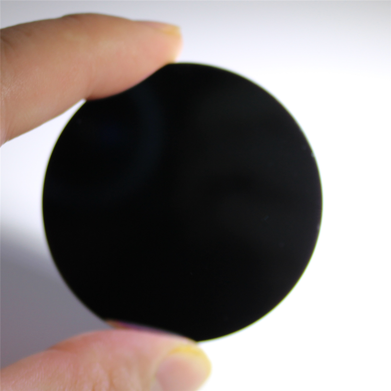
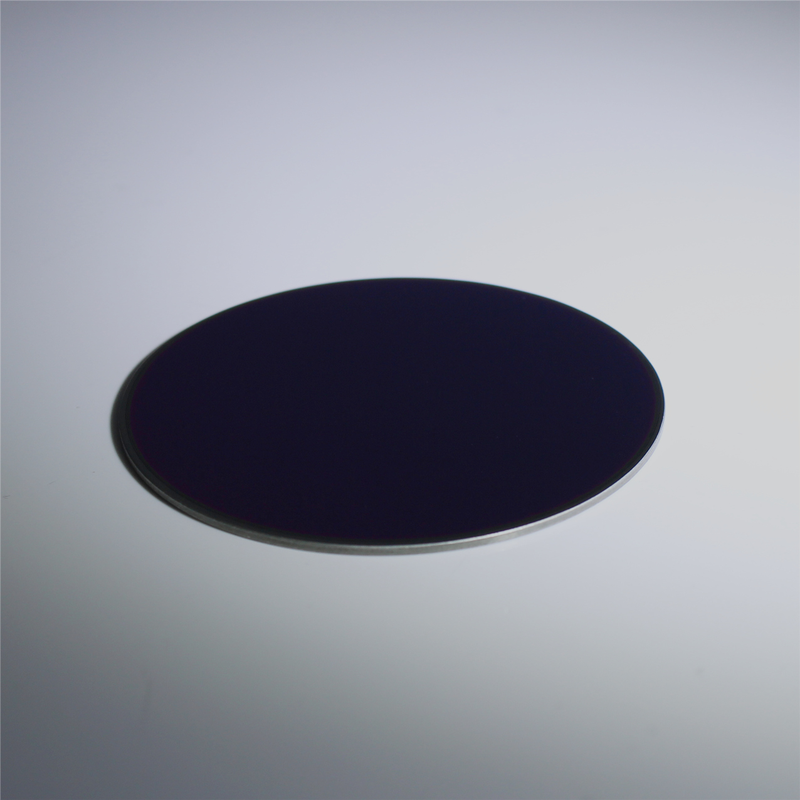
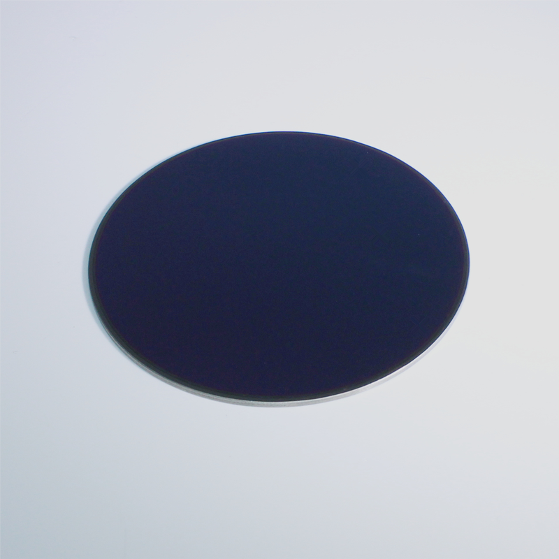
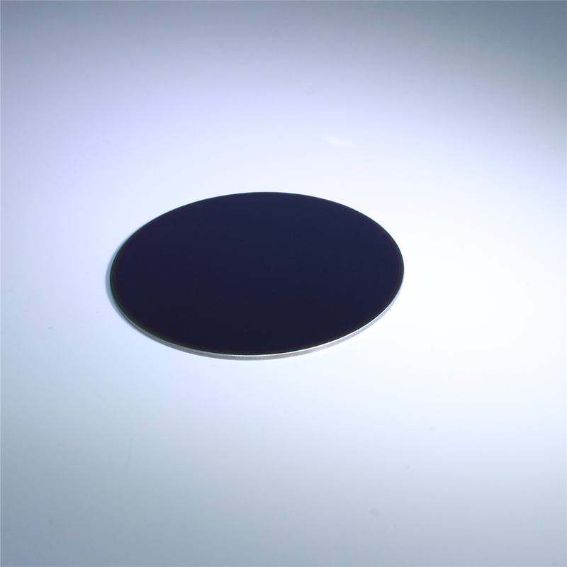
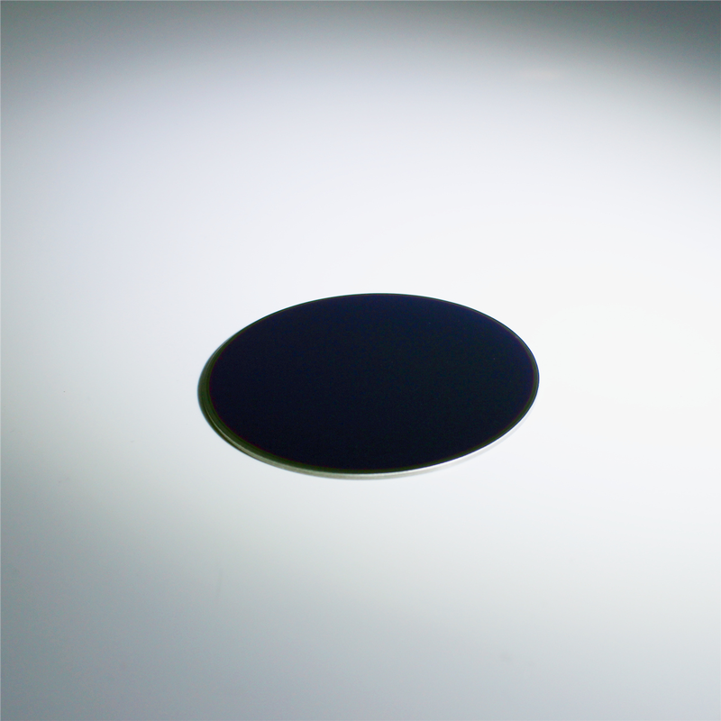
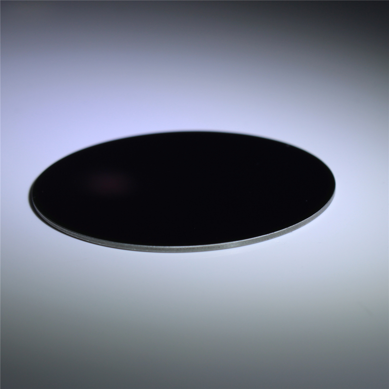
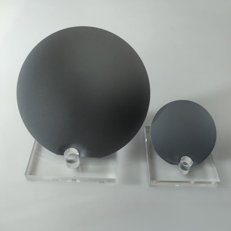
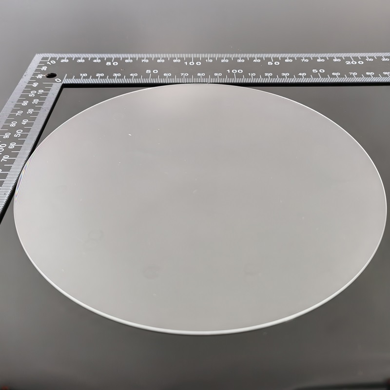
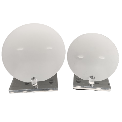
D55mm*T1mm Si (Silicon) Wafer with AR coating @7-14 um VY_20B2T64Si
Material: Silicon Dimension: Dia.55mm Thickness: 1.00mm Tolerance : +/-0.10mm Silicon wafers are a key component of integrated circuits such as those used to power computers, cellphones, and a wide variety of other devices. A silicon wafer (Si wafer) consists of a thin slice of silicon which can be treated in various ways, depending on the type of electronics it is being used in. Silicon is a very high quality semiconductor, making it ideal for the production of such circuits, although other materials have been explored historically. Question one: What is a Silicon Wafer? To begin we will explain silicon and the characteristics of this element that make it appropriate for our uses. Silicon is the second most common element on Earth and it is the seventh-most common element in the entire universe. It is the most common semi conductor and the most widely used in the electronic and technology sector. There are different silicon fabrication methods including the horizontal gradient freeze method, the horizontal bridgeman method, the vertical bridgeman method, the vertical gradient freeze and finally the Czochralski pulling method. During the growth process intentional additions of dopants can be added to the to change the purity of the silicon depending on what the purpose of it will be. These introduced impurities can change the electrical properties of the silicon, which can be useful depending on what the silicon is ultimately being produced for. Boron, aluminum, nitrogen, gallium and indium are just some of the silicon dopants that can be introduced during the growth process. Depending on what level the silicon has been doped, the semiconductor can be considered extrinsic or degenerate. Extrinsic would be lightly to moderately doped whereas degenerate semiconductors act more as conductors because of the high levels of doping that occurs during the fabrication. Question two: What is a Si Wafer used for? As it was mentioned before, silicon wafer’s primary use is in integrated circuits. Integrated circuits power many of the devices that modern society uses everyday. Computers and smartphones are just two of the devices that are dependent on this technology. Although other semiconductors have been tested overtime, silicon has proved to be stable option. Other uses include sensors, such as the tire pressure sensor system, and solar cells. Silicon wafers absorb the photons in sunlight and this in turn create electricity. Many companies use silicon wafers in their product testing. In this purpose, a lot of time the product or prototype is created and tested. Through this testing the silicon wafer can become damaged and although in the past this would lead to the wafer being discarded and a new wafer being purchased for further testing. With the technology Wafer World has created, however, companies are saving millions! Give us a call at 86-431-84631230 or contact VY Optoelectronics Co.,Ltd. online for all of your wafer needs! We are committed to producing quality wafer products, so contact us freely!
 Save to Favorites
Overview
Datasheet
Please provide your email to download the datasheet.
Invalid email format. Please try again.
Supplier Information
Related Products
-
 Sapphire A-R-M Special Crystal-Orientation Substrate
Optical Material
Jmwafer
A-M-R Orientation Single-Crystal Sapphire Substrate (2~6 Inches) - Material Composition: >99.99%,High Purity, Mono-crystalline Al2O3 (KY) Sapphire A/M/R-Plane Single-Crystal Substrate (2~6 Inches) - End-Face Crystal Orientation [Diameter: 50.8mm]: A-plane (11-20) ± 0.1° Sapphire A/M/R-Plane Single-Crystal Substrate (2~6 Inches) - End-Face Crystal Orientation [Diameter: 100mm]: A-plane (11-20) ± 0.1°
α-Al2O3 Hexagonal Lattice,Chemically Stable/Water-Insoluble/Strong Acid-Alkali Resistant,Mohs9,Melts2050℃/Boils3500℃,Operating up to1900℃,Good Transmission/Thermal Conduction/Insulation/Mechanics,Wear/Scratch Resistance.
-
 N-Type Silicon Carbide Epitaxy
Optical Material
Jmwafer
N-Type Silicon Carbide Epitaxial Substrate (2~8 Inches) - Substrate Diameter: 2 inch - 50.8mm N-Type Silicon Carbide Epitaxial Substrate (2~8 Inches) - Substrate Diameter: 4 inch - 100mm N-Type Silicon Carbide Epitaxial Substrate (2~8 Inches) - Substrate Diameter: 6 inch - 150mm
N-Type SiC Epitaxy Grows N-Doped Layer on SiC,High Electron Mobility/Thermal Conductivity/Breakdown Field.
-
 Silicon-Based GaN Epitaxial Template
Optical Material
Jmwafer
Silicon-Based GaN Epitaxial Template Substrate (2~8 Inches) - Substrate Diameter: 50.8mm Silicon-Based GaN Epitaxial Template Substrate (2~8 Inches) - Substrate Diameter: 100mm Silicon-Based GaN Epitaxial Template Substrate (2~8 Inches) - Substrate Diameter: 150mm
GaN-on-Si Epitaxy Grows GaN Films on Silicon,Combining GaN Performance with Low-Cost Silicon.
-
 High-Borosilicate Glass BF33
Optical Material
Jmwafer
High-Borosilicate Glass - Material: BF33 High-Borosilicate Glass - Diameter: 50.8mm High-Borosilicate Glass - Diameter: 100mm
BF33 Special Borosilicate Glass with Low Expansion,Heat Resistance,Chemical Stability and Excellent Transmission.
-
 Sapphire-Based GaN Epitaxial Template
Optical Material
Jmwafer
Sapphire-Based GaN Epitaxial Template Substrate (2~8 Inches) - Substrate Diameter: 50.8mm Sapphire-Based GaN Epitaxial Template Substrate (2~8 Inches) - Substrate Diameter: 100mm Sapphire-Based GaN Epitaxial Template Substrate (2~8 Inches) - Substrate Diameter: 150mm
GaN-on-Sapphire Epitaxial Template Grows GaN Film on Al₂O₃,Common Substrate for Heat/Chemical Stability/Cost Advantages.
Related Articles
Driven by worldwide energy‑structure transformation, the lithium‑ion battery industry is expanding rapidly as green, high‑efficiency energy‑storage devices gain surging global market demand. With years‑long dedication to intelligent manufacturing, Han’s Laser Lithium‑battery Intelligent Equipment has accumulated solid R&D strength and rich practical experience. By integrating multiple cutting‑edge technologies, the company delivers high‑efficiency, eco‑friendly and sustainable lithium‑ion battery production lines, bringing revolutionary upgrades to the new‑energy battery sector.
A solid-state laser is one of the most common and reliable laser types used in modern industry, medical equipment, and scientific research. Unlike gas or fiber lasers, it uses solid materials as its gain medium to generate stable, high-brightness laser beams. Thanks to its high precision, long lifespan, and compact structure, solid-state lasers have become a mainstream solution for high-precision laser processing and optical systems.
FiDAR, the fiber‑optic radar vehicle positioning and tracking system developed by Jianhe Bafang, is a high‑sensitivity distributed fiber‑sensing solution designed for intelligent traffic road monitoring. It outputs real‑time spatial coordinates of every vehicle across the full road section around‑the‑clock, delivering a brand‑new sensing technology for vehicle‑road cooperation, smart highway construction and urban traffic management.
As a vital emerging sector of modern three-dimensional spatial economy, the low-altitude economy has become a new global growth driver. It covers a wide range of commercial scenarios, including UAV navigation and obstacle avoidance, precise airspace management, aerial mapping, low-altitude logistics distribution, security monitoring and emergency disaster rescue. Nevertheless, frequent extreme weather, complex terrain obstacles and increasingly dense low-altitude flight activities pose severe challenges to the safety and stability of low-altitude aircraft operations.
Loading...
Name
Phone
Organization
Use Case

Database Platform