
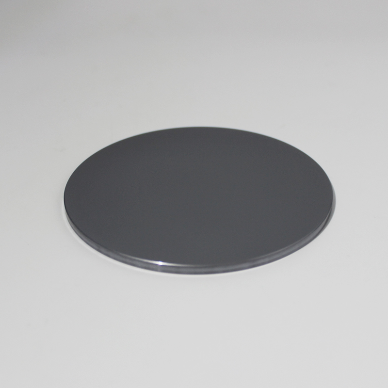
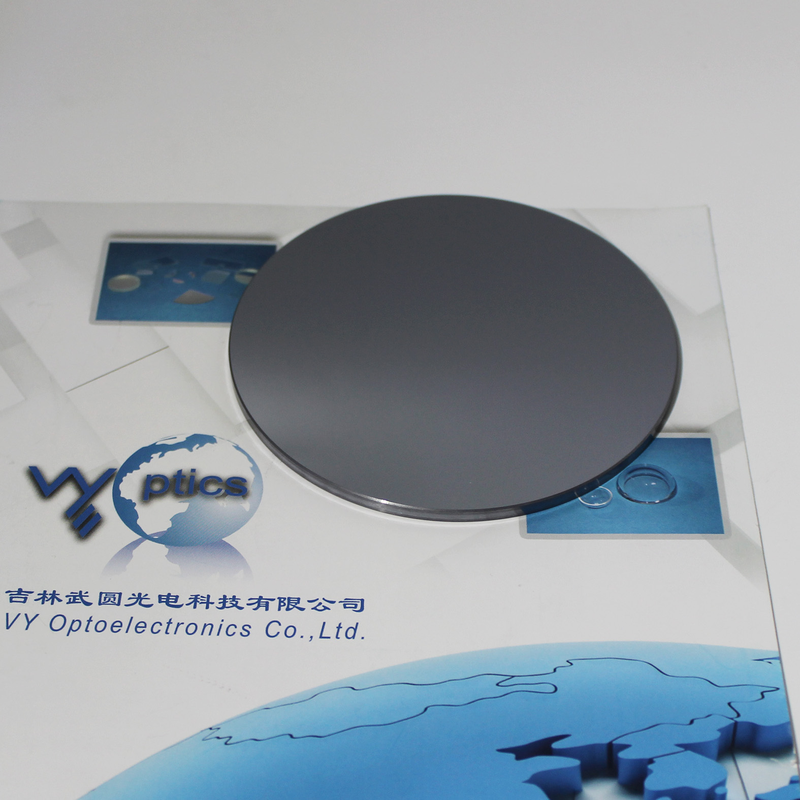
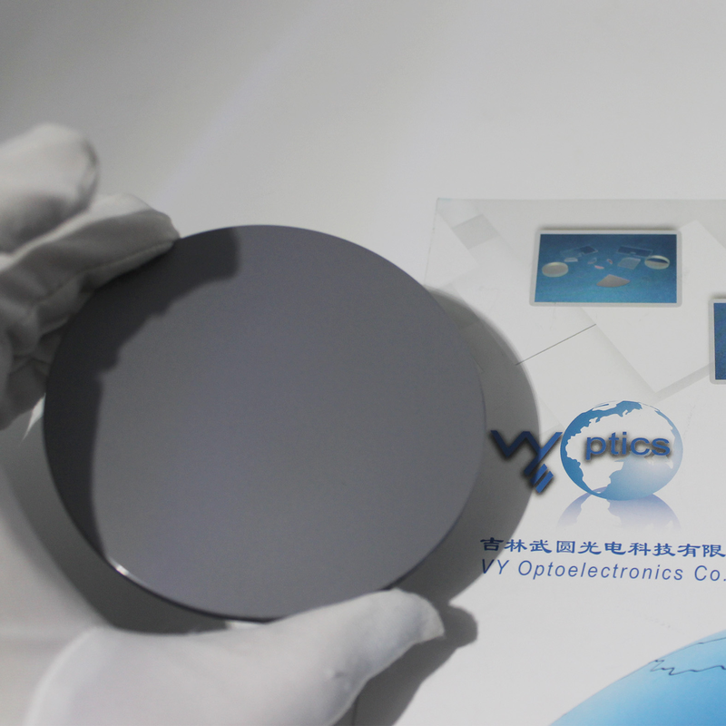
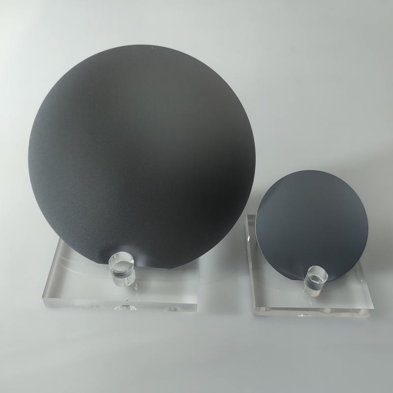
Custom High Purity P Type Dopant Single Side Polished Silicon Wafer X-P24Z2L1202
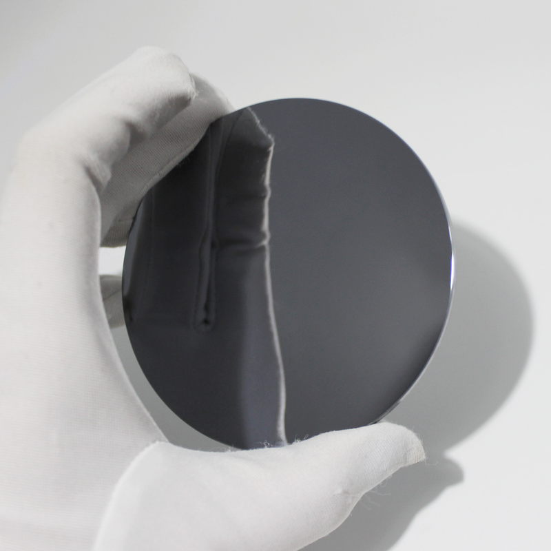
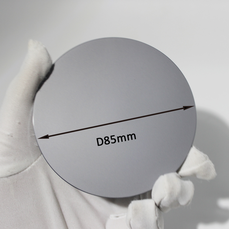
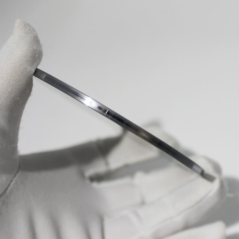
A silicon wafer is a material essential for manufacturing semiconductors, which are found in all kinds of electronic devices that enrich our lives.Few of us have a chance to encounter an actual silicon wafer in daily life. This ultra-flat disk is polished to a mirror-like surface, and made as free as possible of tiny surface irregularities, making it the flattest object in the world. It is also ultra-clean, virtually free of microparticles and other impurities. These qualities are necessary so it can be used as the substrate material of today’s state-of-the-art semiconductors. Silicon wafer is a material used for producing semiconductors, which can be found in all types of electronic devices that improve the lives of people. Silicon comes second as the most common element in the universe; it is mostly used as a semiconductor in the technology and electronic sector. Most people have had the chance to encounter a real silicon wafer in their life. This super-flat disk is refined to a mirror-like surface. Besides, it is also made of subtle surface irregularities which make it the flattest object worldwide. Material: Silicon Dimension: Dia. 85.00mm Thickness: 3.00mm Tolerance : +/-0.10mm
 Save to Favorites
Overview
Specifications
| Parameter | Value |
|---|---|
| Diameter | 85mm |
| Thickness | 3mm |
| Growth Method | CZ |
| Orientation | <100> |
| P Type Dopant | Typtical Boron |
| Resistivity | 0.001~0.005Ω |
| TTV | <10um |
| Polished Surface | Single Side |
Applications
Datasheet
Please provide your email to download the datasheet.
Invalid email format. Please try again.
Supplier Information
Related Products
-
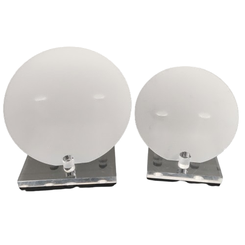 Sapphire A-R-M Special Crystal-Orientation Substrate
Optical Material
Jmwafer
A-M-R Orientation Single-Crystal Sapphire Substrate (2~6 Inches) - Material Composition: >99.99%,High Purity, Mono-crystalline Al2O3 (KY) Sapphire A/M/R-Plane Single-Crystal Substrate (2~6 Inches) - End-Face Crystal Orientation [Diameter: 50.8mm]: A-plane (11-20) ± 0.1° Sapphire A/M/R-Plane Single-Crystal Substrate (2~6 Inches) - End-Face Crystal Orientation [Diameter: 100mm]: A-plane (11-20) ± 0.1°
α-Al2O3 Hexagonal Lattice,Chemically Stable/Water-Insoluble/Strong Acid-Alkali Resistant,Mohs9,Melts2050℃/Boils3500℃,Operating up to1900℃,Good Transmission/Thermal Conduction/Insulation/Mechanics,Wear/Scratch Resistance.
-
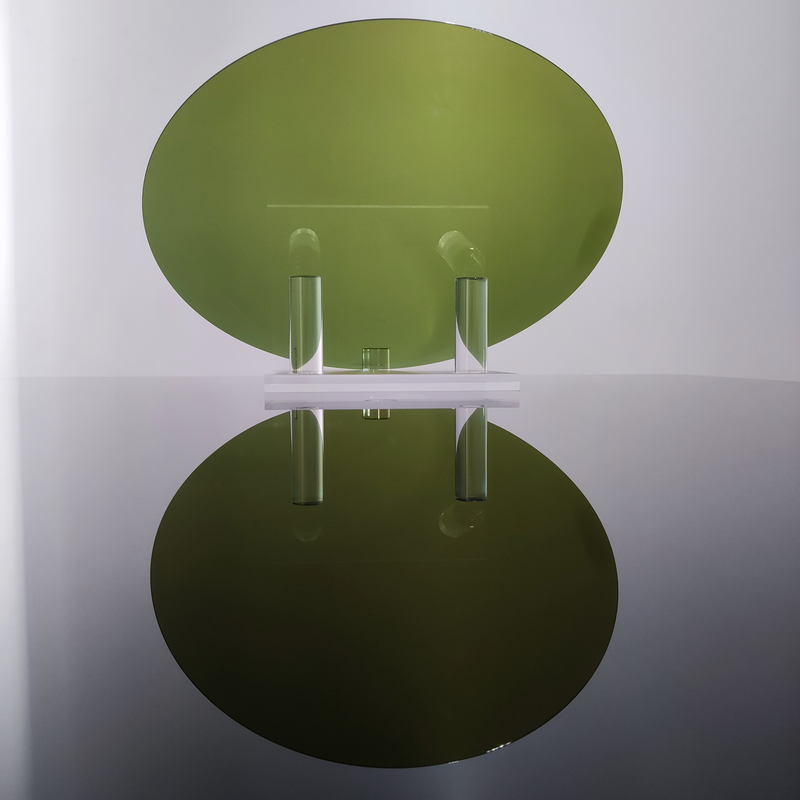 N-Type Silicon Carbide Epitaxy
Optical Material
Jmwafer
N-Type Silicon Carbide Epitaxial Substrate (2~8 Inches) - Substrate Diameter: 2 inch - 50.8mm N-Type Silicon Carbide Epitaxial Substrate (2~8 Inches) - Substrate Diameter: 4 inch - 100mm N-Type Silicon Carbide Epitaxial Substrate (2~8 Inches) - Substrate Diameter: 6 inch - 150mm
N-Type SiC Epitaxy Grows N-Doped Layer on SiC,High Electron Mobility/Thermal Conductivity/Breakdown Field.
-
 Silicon-Based GaN Epitaxial Template
Optical Material
Jmwafer
Silicon-Based GaN Epitaxial Template Substrate (2~8 Inches) - Substrate Diameter: 50.8mm Silicon-Based GaN Epitaxial Template Substrate (2~8 Inches) - Substrate Diameter: 100mm Silicon-Based GaN Epitaxial Template Substrate (2~8 Inches) - Substrate Diameter: 150mm
GaN-on-Si Epitaxy Grows GaN Films on Silicon,Combining GaN Performance with Low-Cost Silicon.
-
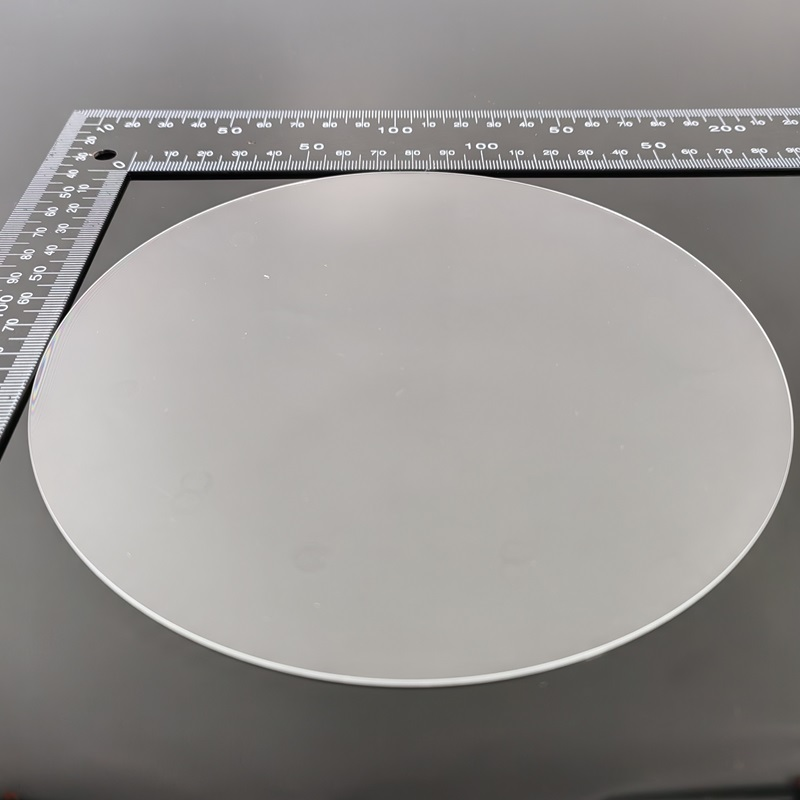 High-Borosilicate Glass BF33
Optical Material
Jmwafer
High-Borosilicate Glass - Material: BF33 High-Borosilicate Glass - Diameter: 50.8mm High-Borosilicate Glass - Diameter: 100mm
BF33 Special Borosilicate Glass with Low Expansion,Heat Resistance,Chemical Stability and Excellent Transmission.
-
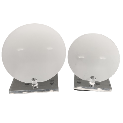 Sapphire-Based GaN Epitaxial Template
Optical Material
Jmwafer
Sapphire-Based GaN Epitaxial Template Substrate (2~8 Inches) - Substrate Diameter: 50.8mm Sapphire-Based GaN Epitaxial Template Substrate (2~8 Inches) - Substrate Diameter: 100mm Sapphire-Based GaN Epitaxial Template Substrate (2~8 Inches) - Substrate Diameter: 150mm
GaN-on-Sapphire Epitaxial Template Grows GaN Film on Al₂O₃,Common Substrate for Heat/Chemical Stability/Cost Advantages.
Related Articles
Developed by RealLight (Beijing), the R7M high‑power diode laser module belongs to the AW multi‑functional laser product family.
VCSEL, short for Vertical Cavity Surface Emitting Laser, is a widely used semiconductor laser component in modern optoelectronics. Unlike traditional edge-emitting lasers, VCSEL emits laser light vertically from its chip surface. Thanks to its low power consumption, stable beam quality, low cost, and easy integration, it has become the core light source for 3D sensing, wearable devices, and high-speed optical communication.
Fomoptic delivers integrated one‑stop optical solutions covering precision optical fabrication and custom vacuum coating services. Supported by complete processing production lines, comprehensive metrology equipment and experienced engineering team, we provide full‑chain customized components, ranging from blank shaping, ultra‑precision polishing to thin‑film coating, for laser systems, infrared imaging, industrial optics and scientific‑research projects.
For pulsed laser and full-spectrum optical testing, photodiodes and thermopiles have inherent drawbacks. Photodiodes show weak response in infrared band, while thermopiles feature slow response and cannot capture nanosecond narrow pulses.
Loading...
Name
Phone
Organization
Use Case

Database Platform