
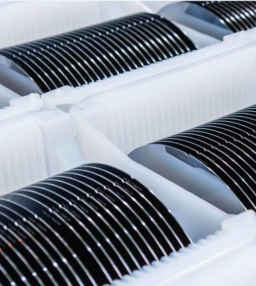


High-performance silicon wafers
Okmetic specializes in advanced silicon wafers tailored for MEMS, RF, and power devices, offering high resistivity and customizable solutions.
 Save to Favorites
Overview
Specifications
| Parameter | Value |
|---|---|
| Wafer Size | 150-200mm |
| Resistivity Range | <0.001Ωcm to >10kΩcm |
| Device Layer Thickness | 1μm to >200μm |
| Buried Oxide Layer Thickness | 0.3μm to 4μm |
| Handle Wafer Thickness | 300μm to 950μm |
| Crystal Material | MCz, A-MCz |
| Wafer Type | SOI, C-SOI, E-SOI, BSOI, DSP, SSP, TSV |
| Surface Flatness | Ultra-flat |
| Wafer Customization Options | Dopants |
| Wafer Customization Options | orientations |
| Wafer Customization Options | resistivities |
Applications
Key Features
Datasheet
Supplier Information
Related Products
-
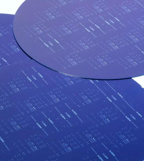 High-performance silicon wafers
Semiconductor Manufacturing Equipment
Ybsemi-Solution
High-performance silicon wafers
Semiconductor Manufacturing Equipment
Ybsemi-Solution
Wafer Size: 150-200mm Resistivity Range: <0.001Ωcm to >10kΩcm Device Layer Thickness: 1μm to >200μm
Okmetic specializes in advanced silicon wafers tailored for MEMS, RF, and power devices, offering high resistivity and customizable solutions.
-
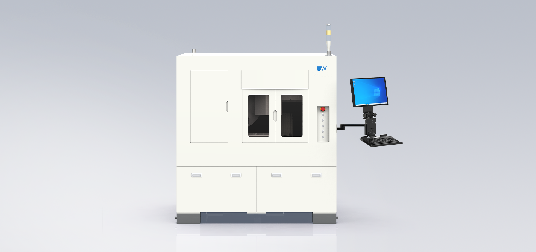 Wafer Scribing Machine
Semiconductor Manufacturing Equipment
Uwlaser
Wafer Scribing Machine
Semiconductor Manufacturing Equipment
Uwlaser
: Parameter value : ≤ 10μm (factory parallelism/flatness/verticality/right angle) : ±0.5μm
-
 Wafer Cleaving System
Semiconductor Manufacturing Equipment
Uwlaser
Wafer Cleaving System
Semiconductor Manufacturing Equipment
Uwlaser
: 2 inch-6 inch wafer : About 2 dollars/s : ±3μm
-
 Laser Wafer Modification Cutting System
Semiconductor Manufacturing Equipment
Uwlaser
Laser Wafer Modification Cutting System
Semiconductor Manufacturing Equipment
Uwlaser
: 4inch, 6inch, 8inch, 12inch (optional) : Maximum 1000mm/s : wafer Frame
-
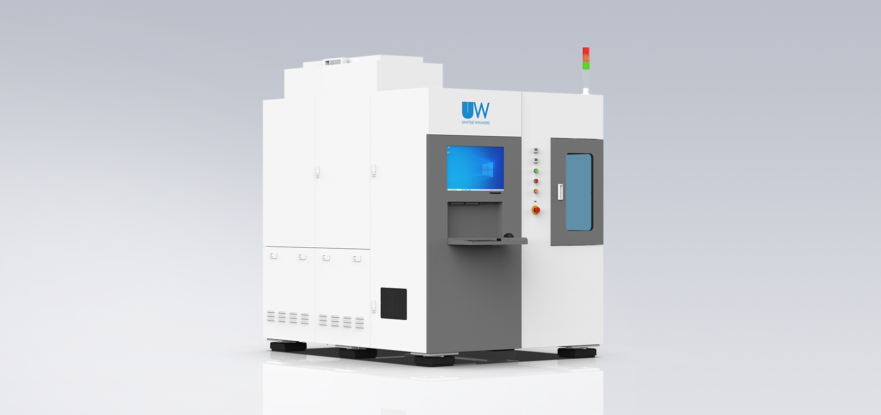
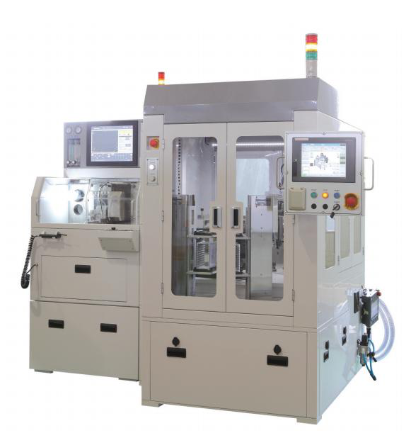 Fully Automatic Optoelectronic Device Die Bonding and Assembly System
Semiconductor Manufacturing Equipment
Ybsemi-Solution
Fully Automatic Optoelectronic Device Die Bonding and Assembly System
Semiconductor Manufacturing Equipment
Ybsemi-Solution
Equipment Type: Fully automatic die bonding and assembly system Configuration: Dual-station enclosed chamber with front double doors Observation Window: Large transparent safety windows on processing chamber
This is a fully automatic high-precision die bonding and assembly system designed for optoelectronic device manufacturing. Based on the product image, the equipment features a dual-station enclosed processing chamber with large observation windows, dual HMI touchscreen control panels, multi-color tower status lights, and automated cassette/magazine loading for substrates or wafers. The system integrates precision motion control, vision alignment, and automated material handling to achieve high-throughput, high-accuracy die attach, component placement, and packaging processes for photonic and semiconductor devices. The enclosed clean-room-compatible design with safety interlocks ensures process stability, particle control, and operator safety during continuous production.
Related Articles
An infrared transmitter (IR transmitter) is a basic electronic component that sends invisible infrared light signals for short-range wireless control. It is widely used in daily electronics, smart home devices, and industrial equipment due to its low cost, low power consumption, and stable performance.
Wuhan Optical Valley Interlink Technology Co., Ltd. was founded in 2013 by a technical team from Huazhong University of Science and Technology.
Looking for a market-verified 808nm pump laser diode? This guide introduces HAUCORE DM-8E5A-8OD (HGLD-808-COS-D-5W), its core advantages, key specs and mainstream industrial, medical & research applications.
Laser pump sources are the core energy input component of solid-state lasers and laser amplifiers, and their performance directly determines the output power, beam quality and service life of the entire laser system. In scenarios such as industrial processing, scientific research experiments and high-end equipment, improper pump source selection will not only result in substandard system performance, but also bring a series of problems such as rapid device degradation and high operation and maintenance costs. This article sorts out the core selection logic and key pitfalls of pump source procurement, and provides selection references based on mature, mass-produced high-reliability products to help purchasers efficiently screen suitable products.
Loading...
Name
Phone
Organization
Use Case

Database Platform