
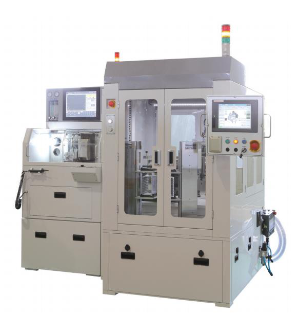
Fully Automatic Optoelectronic Device Die Bonding and Assembly System
This is a fully automatic high-precision die bonding and assembly system designed for optoelectronic device manufacturing. Based on the product image, the equipment features a dual-station enclosed processing chamber with large observation windows, dual HMI touchscreen control panels, multi-color tower status lights, and automated cassette/magazine loading for substrates or wafers. The system integrates precision motion control, vision alignment, and automated material handling to achieve high-throughput, high-accuracy die attach, component placement, and packaging processes for photonic and semiconductor devices. The enclosed clean-room-compatible design with safety interlocks ensures process stability, particle control, and operator safety during continuous production.
 Save to Favorites
Overview
Specifications
| Parameter | Value |
|---|---|
| Equipment Type | Fully automatic die bonding and assembly system |
| Configuration | Dual-station enclosed chamber with front double doors |
| Observation Window | Large transparent safety windows on processing chamber |
| Operator Interface | Dual touchscreen HMI panels |
| Status Indicator | Multi-color tower light (red/yellow/green) |
| Loading/Unloading Method | Automatic cassette/magazine handling |
| Emergency Stop | Equipped with E-stop buttons on both control panels |
| Control Buttons | Start/Stop/Reset push buttons with indicator lamps |
| Pneumatic Interface | External air supply connection with tubing on right side |
| Cabinet | Lower storage cabinets with ventilation and lockable doors |
| Safety Interlock | Door interlock switches on chamber doors |
| Operating Environment | Cleanroom-compatible design |
Applications
Key Features
Datasheet
Supplier Information
Related Products
-
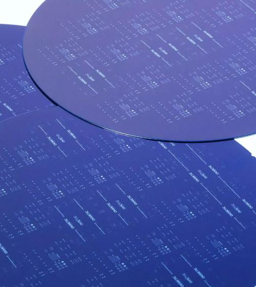 High-performance silicon wafers
Semiconductor Manufacturing Equipment
Ybsemi-Solution
High-performance silicon wafers
Semiconductor Manufacturing Equipment
Ybsemi-Solution
Wafer Size: 150-200mm Resistivity Range: <0.001Ωcm to >10kΩcm Device Layer Thickness: 1μm to >200μm
Okmetic specializes in advanced silicon wafers tailored for MEMS, RF, and power devices, offering high resistivity and customizable solutions.
-
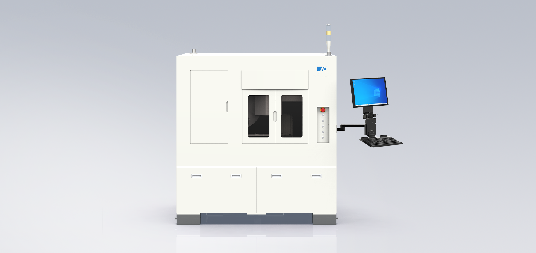 Wafer Scribing Machine
Semiconductor Manufacturing Equipment
Uwlaser
Wafer Scribing Machine
Semiconductor Manufacturing Equipment
Uwlaser
: Parameter value : ≤ 10μm (factory parallelism/flatness/verticality/right angle) : ±0.5μm
-
 Wafer Cleaving System
Semiconductor Manufacturing Equipment
Uwlaser
Wafer Cleaving System
Semiconductor Manufacturing Equipment
Uwlaser
: 2 inch-6 inch wafer : About 2 dollars/s : ±3μm
-
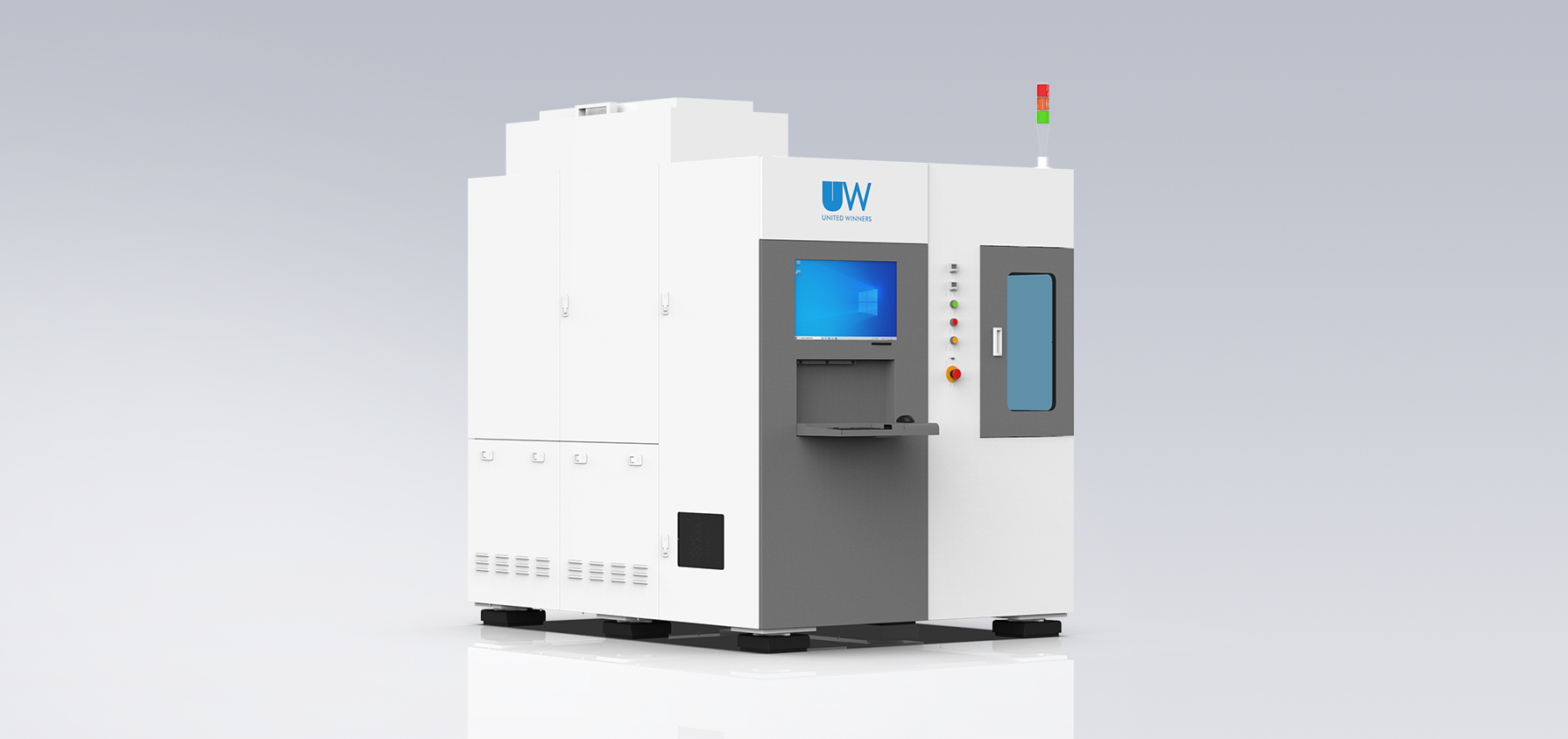 Laser Wafer Modification Cutting System
Semiconductor Manufacturing Equipment
Uwlaser
Laser Wafer Modification Cutting System
Semiconductor Manufacturing Equipment
Uwlaser
: 4inch, 6inch, 8inch, 12inch (optional) : Maximum 1000mm/s : wafer Frame
Related Articles
Electro-optic deflectors (EODs) are optical devices used to steer or deflect light beams by applying an electric field to a specialized optical crystal. Unlike mechanical beam steering systems that rely on moving mirrors, electro-optic deflectors enable high-speed, non-mechanical beam control with exceptional precision and responsiveness. They are widely used in laser scanning, optical communications, microscopy, laser printing, spectroscopy, and scientific research, where rapid and accurate laser beam positioning is essential.
An infrared transmitter (IR transmitter) is a basic electronic component that sends invisible infrared light signals for short-range wireless control. It is widely used in daily electronics, smart home devices, and industrial equipment due to its low cost, low power consumption, and stable performance.
Shanghai Connet Laser Technology Co., Ltd. focuses on technological innovation, delivering cutting-edge photonic products & solutions for industrial lasers, LiDAR, fiber optic sensing, coherent telecom, cold atom physics and precision spectroscopy research & mass manufacturing.
Wuhan Optical Valley Interlink Technology Co., Ltd. was founded in 2013 by a technical team from Huazhong University of Science and Technology.
Loading...
Name
Phone
Organization
Use Case

Database Platform