
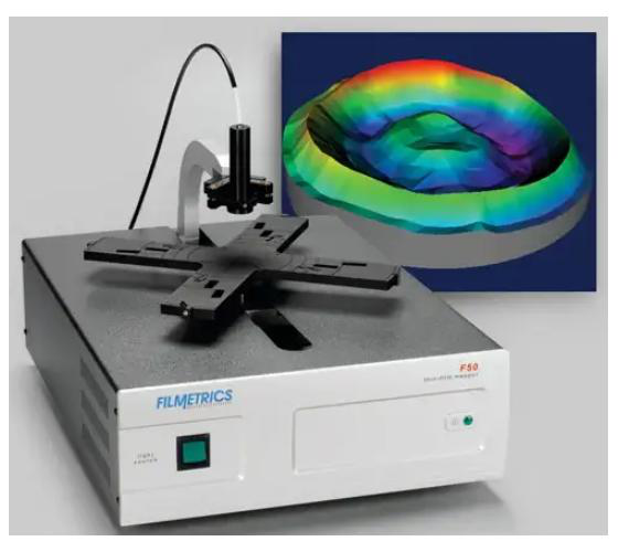
F50 Thin-Film Measurement System
The Filmetrics F50 Thin-Film Measurement System is designed for precise and efficient measurement of thin-film thickness and optical constants. It is ideal for research and industrial applications requiring high accuracy and repeatability.
 Save to Favorites
Overview
Specifications
| Parameter | Value |
|---|---|
| Measurement Range | 1nm-70µm |
| Measurement Accuracy | ±0.4nm |
| Spectral Range | 380nm-1050nm |
| Measurement Speed | <1s per point |
| Sample Size | Up to 200mm |
| Data Interface | USB |
| Data Interface | Ethernet |
| Software Support | Windows-based analysis software |
Applications
Key Features
Datasheet
Supplier Information
Related Products
-
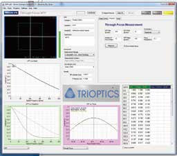 Optical Measurement Software
Optical Metrology
ColorSpace
Optical Measurement Software
Optical Metrology
ColorSpace
Measurement Accuracy: High precision Supported Wavelength Range: Wide range Data Analysis Functions: Comprehensive
A high-precision optical measurement software designed for analyzing and evaluating optical systems.
-
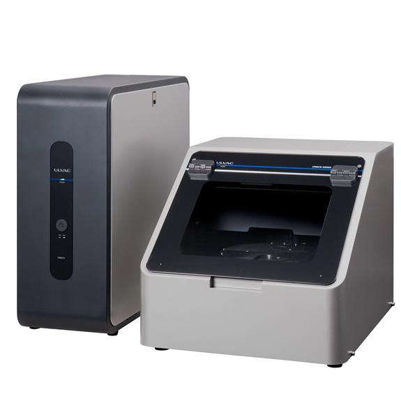 膜厚测量仪
Optical Metrology
UlvacShanghai
膜厚测量仪
Optical Metrology
UlvacShanghai
Model: 1500A, 2000A, 3000A Wavelength Range: 530~750nm, 380~760nm (optional) Spot Diameter: φ1mm, φ0.3mm (optional)
The ULVAC膜厚测量仪 is a high-precision optical measurement device designed for thin film thickness analysis, offering automated measurement capabilities and advanced control systems.
-
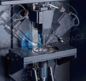 Unknown
Optical Metrology
ColorSpace
Unknown
Optical Metrology
ColorSpace
Operating Voltage: Unknown Power: Unknown Accuracy: Unknown
This product appears to be a high-precision optical device, likely used for advanced measurement or manufacturing processes.
-
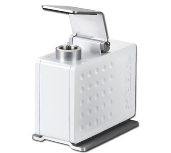 Filmetrics F3-CS Compact Thin-Film Thickness Measurement System
Optical Metrology
Ybsemi-Solution
Filmetrics F3-CS Compact Thin-Film Thickness Measurement System
Optical Metrology
Ybsemi-Solution
Measurement Principle: Spectral Reflectance Film Thickness Range: 15nm-75μm Wavelength Range: 380-1050nm
The Filmetrics F3-CS is a compact benchtop thin-film thickness measurement system based on spectral reflectance. Light reflected from the top and bottom interfaces of a film stack generates an interference spectrum, which is captured by the built-in spectrometer and fitted by the FILMeasure software against an extensive material library to report film thickness and optical constants (n and k) in under a second. The top-loading sample port with a flip-up cover makes measurement fast and repeatable, while the non-contact optical technique never touches or damages the sample. Covering a typical thickness range of 15nm to 75μm, the F3-CS handles dielectrics, photoresists, polymers and other transparent or semi-transparent films, offering an affordable, easy-to-use alternative to spectroscopic ellipsometers for R&D, failure analysis and production quality control.
-
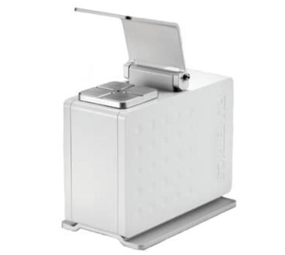 Benchtop Thin-Film Thickness Analyzer (Spectroscopic Reflectometer)
Optical Metrology
Ybsemi-Solution
Benchtop Thin-Film Thickness Analyzer (Spectroscopic Reflectometer)
Optical Metrology
Ybsemi-Solution
Measurement Principle: Spectral reflectance Thickness Measurement Range: 15Å–70µm Wavelength Range: 380–1050nm
A compact benchtop optical metrology system designed for fast, non-contact and non-destructive thickness measurement of transparent and semi-transparent thin films. Based on the image, the instrument integrates a manual sample stage with a vacuum chuck, an enclosed optical measurement head protected by a flip-up cover, and a single-box architecture that is easy to deploy in laboratories, cleanrooms and production lines. Working on the principle of spectral reflectance, the system illuminates the sample with broadband light, collects the reflected interference spectrum with a built-in spectrometer, and calculates film thickness by fitting the spectrum against a materials library of refractive index (n & k) data. It measures single-layer and multilayer stacks such as oxides, nitrides, photoresists, ITO, anti-reflection coatings and polymer films on wafers, glass or metal substrates, delivering results in seconds without any sample preparation.
Related Articles
Electro-optic deflectors (EODs) are optical devices used to steer or deflect light beams by applying an electric field to a specialized optical crystal. Unlike mechanical beam steering systems that rely on moving mirrors, electro-optic deflectors enable high-speed, non-mechanical beam control with exceptional precision and responsiveness. They are widely used in laser scanning, optical communications, microscopy, laser printing, spectroscopy, and scientific research, where rapid and accurate laser beam positioning is essential.
An infrared transmitter (IR transmitter) is a basic electronic component that sends invisible infrared light signals for short-range wireless control. It is widely used in daily electronics, smart home devices, and industrial equipment due to its low cost, low power consumption, and stable performance.
Shanghai Connet Laser Technology Co., Ltd. focuses on technological innovation, delivering cutting-edge photonic products & solutions for industrial lasers, LiDAR, fiber optic sensing, coherent telecom, cold atom physics and precision spectroscopy research & mass manufacturing.
Wuhan Optical Valley Interlink Technology Co., Ltd. was founded in 2013 by a technical team from Huazhong University of Science and Technology.
Loading...
Name
Phone
Organization
Use Case

Database Platform