






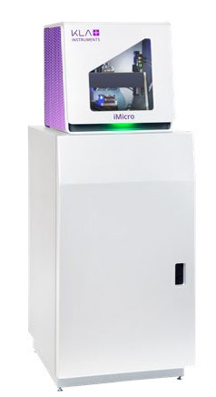
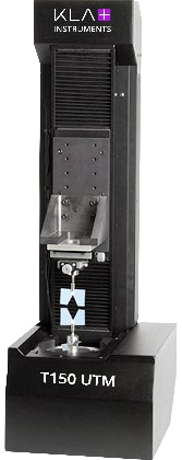
NanoFlip
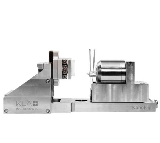
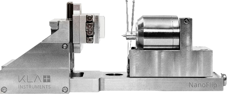
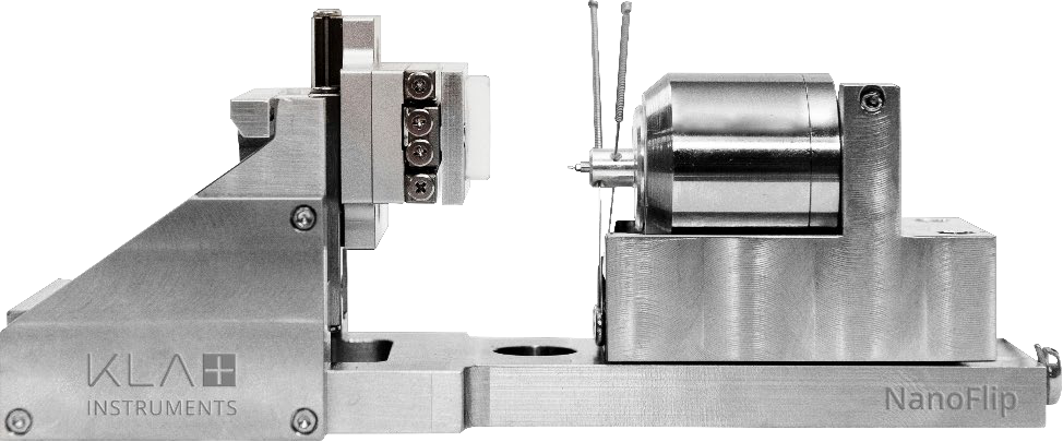
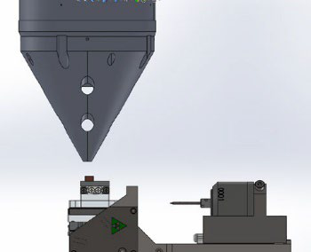
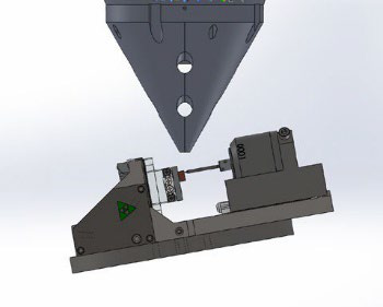
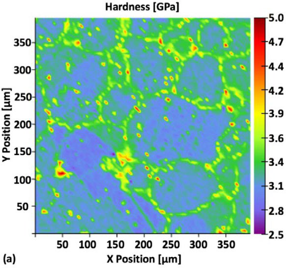
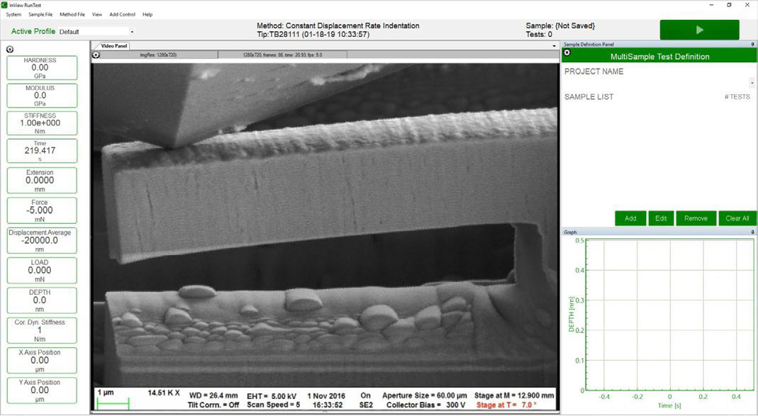
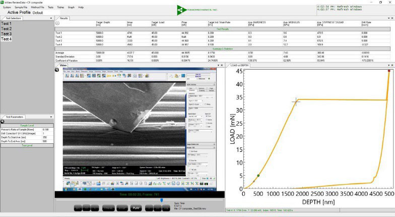
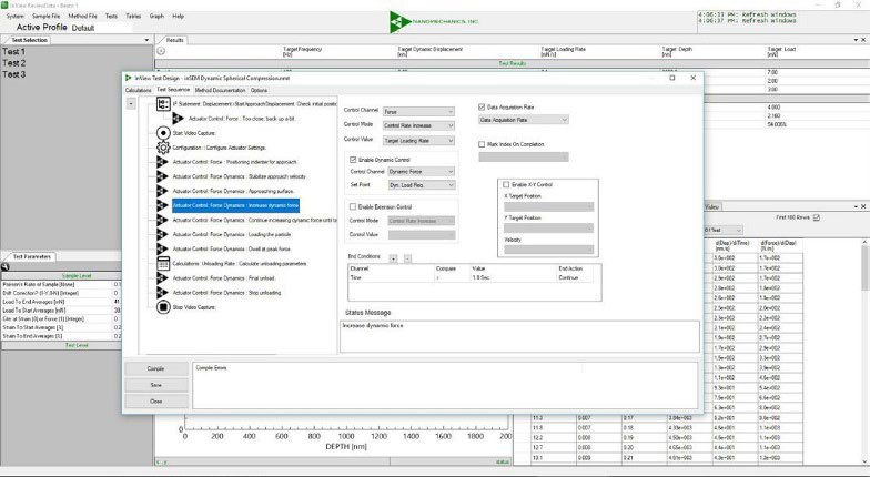
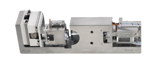
NanoFlip is a versatile nanomechanical testing instrument equipped with a flip mechanism, enabling seamless switching between imaging and testing. It is designed for precise material property analysis and supports various testing scenarios.
 Save to Favorites
Overview
Specifications
| Parameter | Value |
|---|---|
| Magnetic Force Sensor | InForce 50 |
| Indentation Depth | up to 50μm |
| Electromagnetic Force Range | 50mN |
| Indentation Frequency | up to 100kHz |
| International Standard | ISO 14577 |
| Video Capture Frequency | up to 1kHz |
| Flip Angle | 90° |
| Synchronized Video Capture | Available |
| User-defined Testing Protocol | Supported |
| Data Acquisition Mode | DataBurst mode |
| Mechanical Property Scanning | NanoBlitz 4D |
| Indenter Type | Various shapes supported |
| Sample Base | Easy to install |
| Compatibility with Optical Profilometers | Filmetrics Profilom3D and Zeta-20 |
| Software Features | InView |
| Software Features | RunTest |
| Software Features | ReviewData |
| Software Features | InFocus |
Applications
Key Features
Datasheet
Supplier Information
Related Products
-
 SU8600 Series Scanning Electron Microscope
Material Analysis and Forensics
Ybsemi-Solution
SU8600 Series Scanning Electron Microscope
Material Analysis and Forensics
Ybsemi-Solution
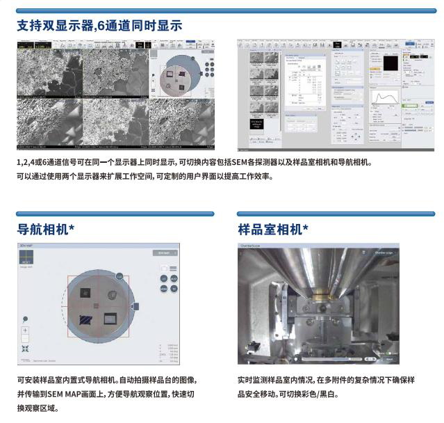
Secondary Electron Resolution: 0.6nm@15kV, 0.7nm@1kV Magnification: 20-2,000,000× Electron Gun: 冷阴极场发射枪, 支持技术间活动Function, Includes 低噪声模块系统
The SU8600 series scanning electron microscope offers high-resolution imaging and advanced analytical capabilities, suitable for various applications in materials science, semiconductor inspection, and biological research.
-
 PHEMOS-X
Material Analysis and Forensics
Ybsemi-Solution
PHEMOS-X
Material Analysis and Forensics
Ybsemi-Solution
Main Unit Dimensions: 1656mm(W)×2000mm(H)×1247mm(D) Main Unit Weight: Approx.1640kg Operation Desk Dimensions 1: 1000mm(W)×700mm(H)×800mm(D)
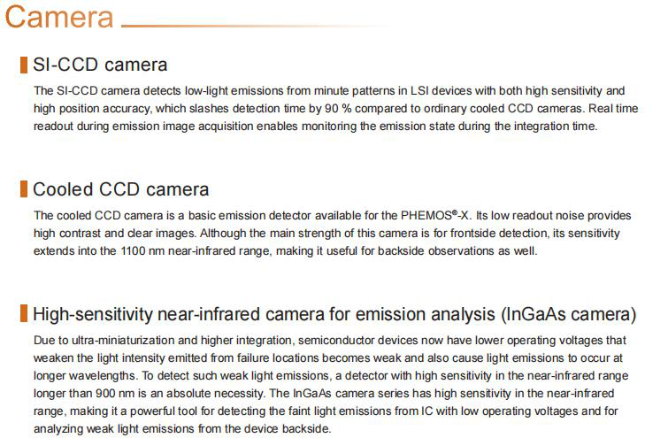
PHEMOS-X is a high-performance emission analysis system designed for detecting low-light emissions from semiconductor devices with high sensitivity and precision. It features advanced cameras, display functions, and optical stage capabilities.
-
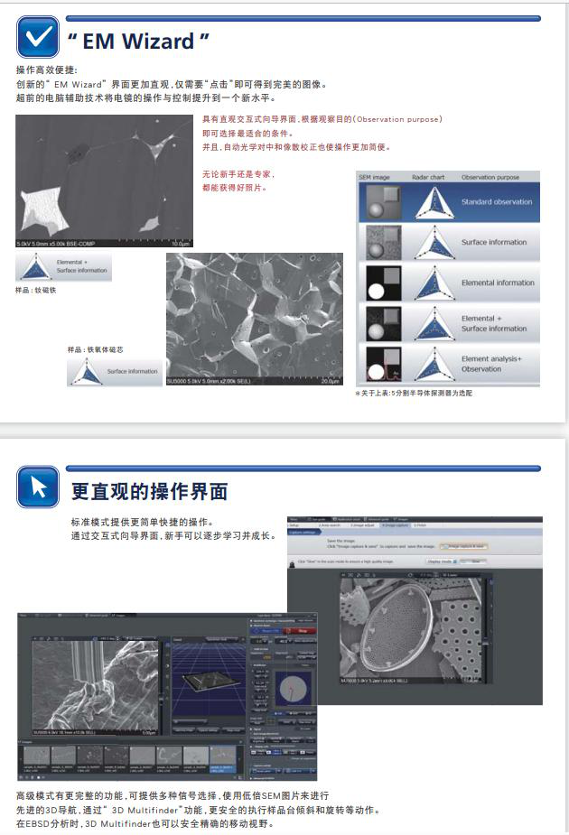 SU5000 Scanning Electron Microscope
Material Analysis and Forensics
Ybsemi-Solution
SU5000 Scanning Electron Microscope
Material Analysis and Forensics
Ybsemi-Solution
Resolution 1.2nm@30kV(SE): 1.2nm Resolution 3.0nm@1kV(SE): 3.0nm Resolution 2.0nm@1kV(SE): 2.0nm
The SU5000 Scanning Electron Microscope (SEM) offers advanced imaging capabilities with intuitive operation, enabling users to achieve high-quality images efficiently.
-
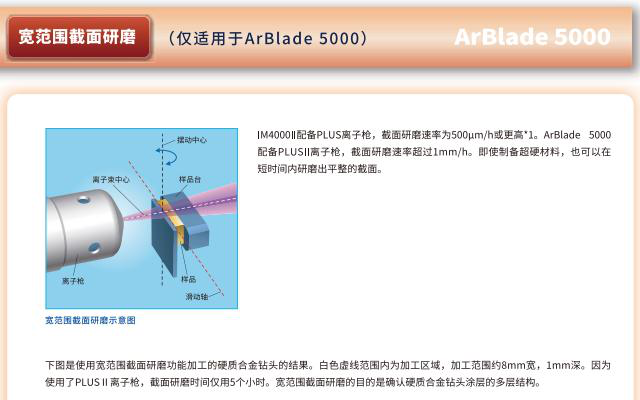 IM4000 II & ArBlade 5000
Material Analysis and Forensics
Ybsemi-Solution
IM4000 II & ArBlade 5000
Material Analysis and Forensics
Ybsemi-Solution
Gas Source: 氩气 Gas Flow Control Method: 质量流量控制 Acceleration Voltage: IM4000 II: 0.0~6.0kV, ArBlade 5000: 0.0~8.0kV
IM4000 II and ArBlade 5000 are advanced ion milling systems designed for precise surface preparation and analysis. They offer high-speed milling capabilities and versatile applications for various materials.
-
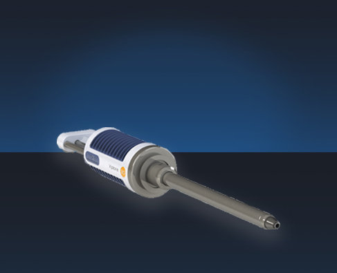 Unknown
Material Analysis and Forensics
Kyky
Unknown
Material Analysis and Forensics
Kyky
Unknown Parameter: Unknown
This is a high-precision optical device designed for specialized applications, offering advanced performance and reliability.
Related Articles
Founded in 2004, Wuhan Union Optic Inc. is a National Specialized, Refined, Unique & Innovative "Little Giant" high-tech enterprise located in Wuhan East Lake High-Tech Development Zone.
Semiconductor laser diodes are essential light sources for industrial sensing, LiDAR and laser printing. Many engineers waste time picking mismatched models. We summarize 4 simple selection standards, plus a mature industrial product: HGLD-790TO5.6-ZSP-10mW from HAUCORE.
Electro-optic deflectors (EODs) are optical devices used to steer or deflect light beams by applying an electric field to a specialized optical crystal. Unlike mechanical beam steering systems that rely on moving mirrors, electro-optic deflectors enable high-speed, non-mechanical beam control with exceptional precision and responsiveness. They are widely used in laser scanning, optical communications, microscopy, laser printing, spectroscopy, and scientific research, where rapid and accurate laser beam positioning is essential.
In photonics and laser technology, devices that manipulate optical signals via the electro-optic effect form the backbone of precision optical systems. Electro-optic phase modulators and electro-optic deflectors are two prominent examples of this device category. As a critical hardware solution for high-speed, high-accuracy laser beam direction control, electro-optic deflectors are widely deployed across industrial and research settings. Below is a detailed overview of their core structure, key performance drivers, and primary use cases.
Loading...
Name
Phone
Organization
Use Case

Database Platform