
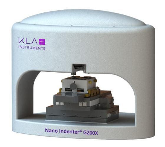


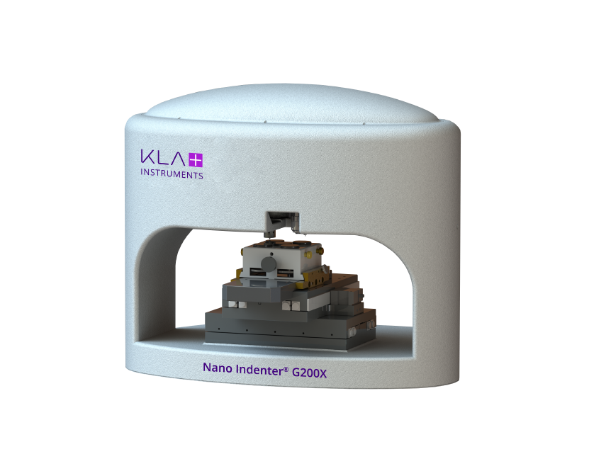


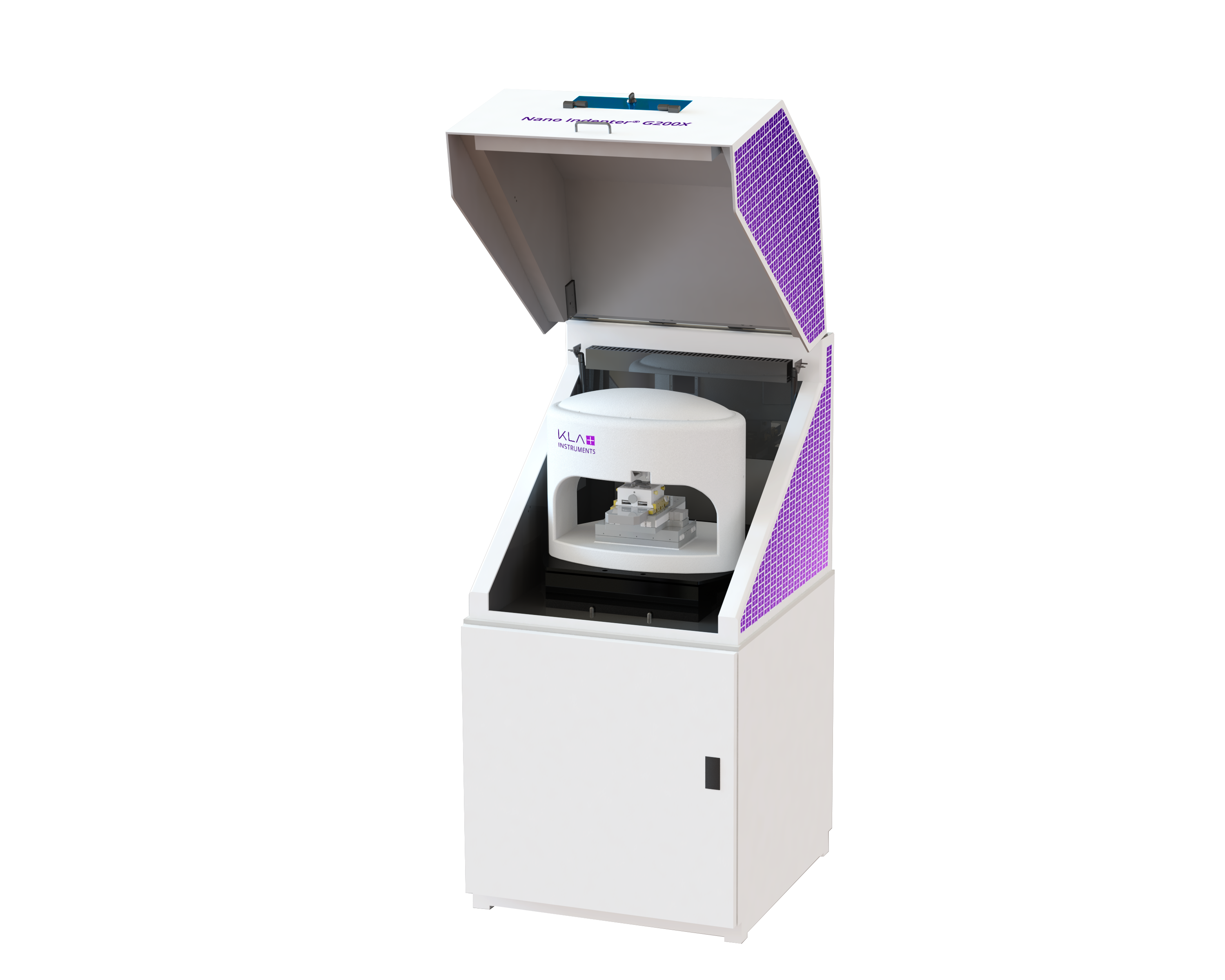

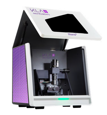
Nano Indenter® G200X
Nano Indenter® G200X is a flexible and user-friendly nano-mechanical testing instrument designed for precise force and displacement measurements from micro to nano scales.
 Save to Favorites
Overview
Specifications
| Parameter | Value |
|---|---|
| Maximum Force | 1000mN |
| Force Resolution | <1nN |
| Displacement Resolution | <0.01nm |
| Maximum Indentation Depth | 500μm |
| Temperature range | Room temperature to 300°C |
| Data Acquisition Rate | 100kHz |
| Indenter Type | Berkovich |
| Indenter Type | Cube Corner |
| Indenter Type | Spherical |
| Indenter Type | Flat Punch |
| Continuous Stiffness Measurement Range | Up to 1000mN |
| Thin Film Thickness Measurement Range | <10nm |
| Scanning Range | 30×30μm to 300×300μm |
| Measurement Accuracy | High precision (X,Y) optical encoder platform |
| Objective Magnification | Up to 100× |
Applications
Key Features
Datasheet
Supplier Information
Related Products
-
 SU8600 Series Scanning Electron Microscope
Material Analysis and Forensics
Ybsemi-Solution
SU8600 Series Scanning Electron Microscope
Material Analysis and Forensics
Ybsemi-Solution
Secondary Electron Resolution: 0.6nm@15kV, 0.7nm@1kV Magnification: 20-2,000,000× Electron Gun: 冷阴极场发射枪, 支持技术间活动Function, Includes 低噪声模块系统
The SU8600 series scanning electron microscope offers high-resolution imaging and advanced analytical capabilities, suitable for various applications in materials science, semiconductor inspection, and biological research.
-
 PHEMOS-X
Material Analysis and Forensics
Ybsemi-Solution
PHEMOS-X
Material Analysis and Forensics
Ybsemi-Solution
Main Unit Dimensions: 1656mm(W)×2000mm(H)×1247mm(D) Main Unit Weight: Approx.1640kg Operation Desk Dimensions 1: 1000mm(W)×700mm(H)×800mm(D)
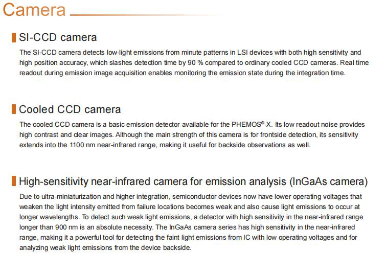
PHEMOS-X is a high-performance emission analysis system designed for detecting low-light emissions from semiconductor devices with high sensitivity and precision. It features advanced cameras, display functions, and optical stage capabilities.
-
 SU5000 Scanning Electron Microscope
Material Analysis and Forensics
Ybsemi-Solution
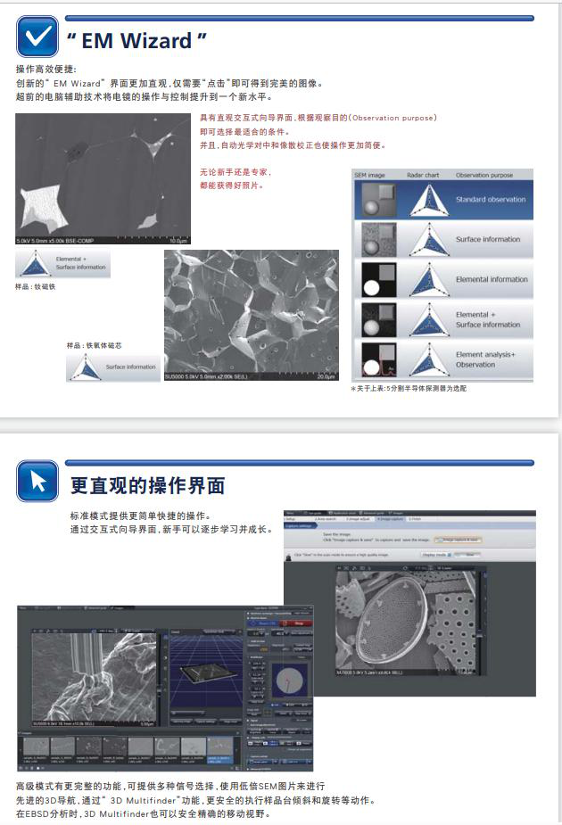
SU5000 Scanning Electron Microscope
Material Analysis and Forensics
Ybsemi-Solution
Resolution 1.2nm@30kV(SE): 1.2nm Resolution 3.0nm@1kV(SE): 3.0nm Resolution 2.0nm@1kV(SE): 2.0nm
The SU5000 Scanning Electron Microscope (SEM) offers advanced imaging capabilities with intuitive operation, enabling users to achieve high-quality images efficiently.
-
 IM4000 II & ArBlade 5000
Material Analysis and Forensics
Ybsemi-Solution
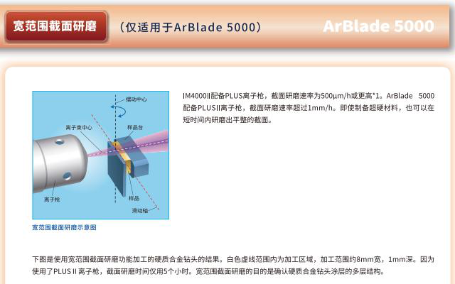
IM4000 II & ArBlade 5000
Material Analysis and Forensics
Ybsemi-Solution
Gas Source: 氩气 Gas Flow Control Method: 质量流量控制 Acceleration Voltage: IM4000 II: 0.0~6.0kV, ArBlade 5000: 0.0~8.0kV
IM4000 II and ArBlade 5000 are advanced ion milling systems designed for precise surface preparation and analysis. They offer high-speed milling capabilities and versatile applications for various materials.
-
 Unknown
Material Analysis and Forensics
Kyky
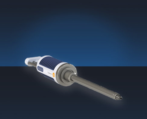
Unknown
Material Analysis and Forensics
Kyky
Unknown Parameter: Unknown
This is a high-precision optical device designed for specialized applications, offering advanced performance and reliability.
Related Articles
Electro-optic deflectors (EODs) are optical devices used to steer or deflect light beams by applying an electric field to a specialized optical crystal. Unlike mechanical beam steering systems that rely on moving mirrors, electro-optic deflectors enable high-speed, non-mechanical beam control with exceptional precision and responsiveness. They are widely used in laser scanning, optical communications, microscopy, laser printing, spectroscopy, and scientific research, where rapid and accurate laser beam positioning is essential.
An infrared transmitter (IR transmitter) is a basic electronic component that sends invisible infrared light signals for short-range wireless control. It is widely used in daily electronics, smart home devices, and industrial equipment due to its low cost, low power consumption, and stable performance.
Shanghai Connet Laser Technology Co., Ltd. focuses on technological innovation, delivering cutting-edge photonic products & solutions for industrial lasers, LiDAR, fiber optic sensing, coherent telecom, cold atom physics and precision spectroscopy research & mass manufacturing.
Wuhan Optical Valley Interlink Technology Co., Ltd. was founded in 2013 by a technical team from Huazhong University of Science and Technology.
Loading...
Name
Phone
Organization
Use Case

Database Platform