
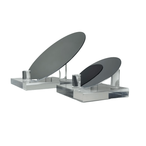
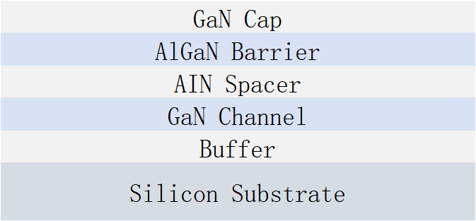
Silicon-Based GaN Epitaxial HEMT
GaN-on-Si HEMT Epitaxy Grows GaN Heterostructures on Silicon for High-Performance High-Electron-Mobility Transistors.
 Save to Favorites
Overview
Specifications
| Parameter | Value |
|---|---|
| Silicon-Based GaN HEMT Epitaxy (2~8 Inches) - Substrate Diameter | 50.8mm |
| Silicon-Based GaN HEMT Epitaxy (2~8 Inches) - Substrate Diameter | 100mm |
| Silicon-Based GaN HEMT Epitaxy (2~8 Inches) - Substrate Diameter | 150mm |
| Silicon-Based GaN HEMT Epitaxy (2~8 Inches) - Substrate Diameter | 200mm |
| Silicon-Based GaN HEMT Epitaxy (2~8 Inches) - Silicon Substrate Thickness [Substrate diameter: 50.8mm] | 1000μm |
| Silicon-Based GaN HEMT Epitaxy (2~8 Inches) - Silicon Substrate Thickness [Substrate diameter: 100mm] | 1000μm |
| Silicon-Based GaN HEMT Epitaxy (2~8 Inches) - Silicon Substrate Thickness [Substrate diameter: 150mm] | 1000μm |
| Silicon-Based GaN HEMT Epitaxy (2~8 Inches) - Silicon Substrate Thickness [Substrate diameter: 200mm] | 1150μm |
| Silicon-Based GaN HEMT Epitaxy (2~8 Inches) - Silicon Substrate Surface | Polished/Etched |
| Silicon-Based GaN HEMT Epitaxy (2~8 Inches) - Silicon Substrate Crystal Orientation | P(111) |
Applications
Datasheet
Please provide your email to download the datasheet.
Invalid email format. Please try again.
Supplier Information
Related Products
-
 Lithium Tantalate Wafer LT
Optical Crystals
Jmwafer
Diameter [Lithium Tantalate Single-Crystal Substrate LiTaO3/LT (2~6 Inches)]: 2 inch - 50.8mm Diameter [Lithium Tantalate Single-Crystal Substrate LiTaO3/LT (2~6 Inches)]: 3 inch - 76.2mm Diameter [Lithium Tantalate Single-Crystal Substrate LiTaO3/LT (2~6 Inches)]: 4 inch - 100mm
LiTaO₃ Usually Colorless/Pale Yellow,Trigonal Distorted-Perovskite Structure,Excellent Electro-Optic,Piezoelectric/Pyroelectric Properties.
-
 Lithium Niobate Wafer LN
Optical Crystals
Jmwafer
Diameter [Lithium Niobate Single-Crystal Substrate LiNbO3/LN (2~6 Inches)]: 2 inch - 50.8mm Diameter [Lithium Niobate Single-Crystal Substrate LiNbO3/LN (2~6 Inches)]: 3 inch - 76.2mm Diameter [Lithium Niobate Single-Crystal Substrate LiNbO3/LN (2~6 Inches)]: 4 inch - 100mm
LiNbO₃ Trigonal,Good Symmetry/Structural Stability,Piezoelectric,Ferroelectric,Photoelectric,Acousto-Optic/Nonlinear Properties,Curie up to1140℃,High Mechanical Quality/Chemical Stability.
-
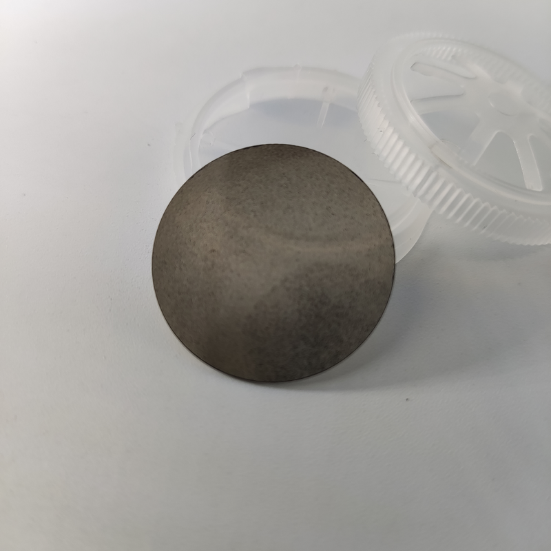 Polycrystalline Diamond
Optical Crystals
Jmwafer
Polycrystalline Diamond - Dimensions: 10 mm × 10 mm Polycrystalline Diamond - Dimensions: 1 inch - 25.4mm Polycrystalline Diamond - Dimensions: 2 inch - 50.8mm
Diamond:Tetrahedrally Packed Carbon,Extremely Hard,Excellent Thermal Conductivity/Broad Optical Transparency,Hardest Known Natural Material,Also Synthesized at High Pressure/Temperature.
-
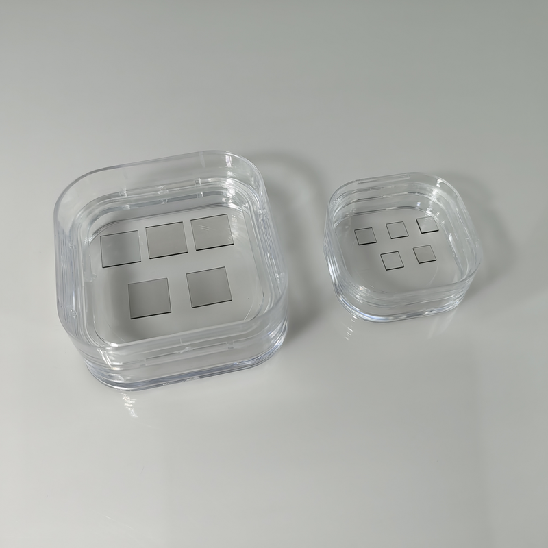 Single-Crystal Diamond
Optical Crystals
Jmwafer
Single-Crystal Diamond - Diameter: 5 mm × 5 mm Single-Crystal Diamond - Diameter: 10 mm × 10 mm Single-Crystal Diamond - Diameter: 20 mm × 20 mm
Diamond:Tetrahedrally Packed Carbon,Extremely Hard,Excellent Thermal Conductivity/Broad Optical Transparency,Hardest Known Natural Material,Also Synthesized at High Pressure/Temperature.
-
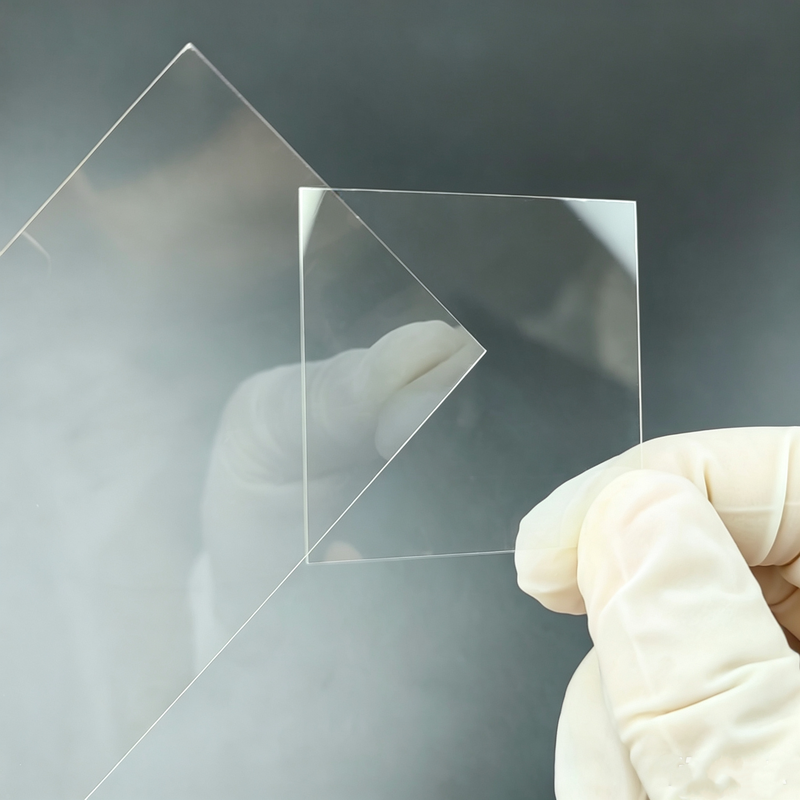 Fluorophlogopite
Optical Crystals
Jmwafer
Fluoromica Substrate - Dimensions: 5 mm × 5 mm Fluoromica Substrate - Dimensions: 10 mm × 10 mm Fluoromica Substrate - Dimensions: 20 mm × 20 mm
Synthetic Fluorophlogopite Mica KMg3(AlSi3O10)F2,Melts1375℃/Long-Term up to1100℃,Colorless Transparent,Strong Acid-Alkali Inert,Stable/Pure/Complete Structure/Flat Cleavage,Easily Split Thin.
Related Articles
Founded in 2003, BWT Beijing Optoelectronics adheres to the mission "Let Dreams Fly With Light" and vision of becoming a Global Leader in Laser Solutions, guided by the core value "Innovate to Achieve Extraordinary".
On January 21, 2026, SPIE Photonics West, one of the world’s leading photonics events, was held in San Francisco, USA. RaySea presented its latest self‑developed VCSEL achievements at this prestigious exhibition. Dr. Lai, the company’s senior R&D representative, delivered a technical speech during the dedicated VCSEL session. His presentation covered cutting‑edge progress of in‑house multi‑junction VCSEL solutions built for automotive lidar and embodied‑intelligence robots, drawing strong attention from the global photonics community.
Shandong Huaguang Optoelectronics Co., Ltd. (HAUCORE) is a leading high-tech manufacturer of compound semiconductor optoelectronic devices, founded in 1999 and headquartered in Jinan, China, with two R&D and production bases in Jinan and Weifang.
Driven by the continuous pursuit of higher precision and efficiency in optical communication and optoelectronic device manufacturing, OLCR-1000 Low-Coherence Interferometer, independently developed by Wuhan Guanggu Interconnect Technology Co., Ltd., provides an innovative technical solution for distributed return loss testing of optical fibers and optoelectronic devices.
Loading...
Name
Phone
Organization
Use Case

Database Platform