RaySea Showcases High‑Performance Multi‑Junction VCSEL Technology at Photonics West
Published: 2026-08-20 10:48:23 Views: 93
On January 21, 2026, SPIE Photonics West, one of the world’s leading photonics events, was held in San Francisco, USA. RaySea presented its latest self‑developed VCSEL achievements at this prestigious exhibition. Dr. Lai, the company’s senior R&D representative, delivered a technical speech during the dedicated VCSEL session. His presentation covered cutting‑edge progress of in‑house multi‑junction VCSEL solutions built for automotive lidar and embodied‑intelligence robots, drawing strong attention from the global photonics community.
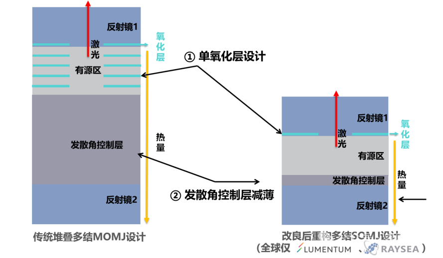
Autonomous‑driving systems and humanoid robots impose strict requirements on lidar sources in terms of detection range, ranging precision and long‑term operational reliability. To meet these demanding market requirements, RaySea has developed the fully‑independent Single‑Oxidation Multiple‑Junction (SOMJ) VCSEL platform. This proprietary technology features five core strengths: superior output power and power density, high‑duty‑cycle operating capability, outstanding electro‑optical conversion efficiency, narrow beam divergence angle and automotive‑grade reliability. It provides an ideal light‑source solution for long‑range lidar deployed under harsh operating conditions.
Leveraging the SOMJ technology foundation, RaySea has built a comprehensive VCSEL product portfolio including single‑point emitters, linear arrays and 1D / 2D addressable area arrays. These optoelectronic chips serve a wide range of applications such as automotive lidar, consumer electronics, service robots, high‑speed data communication, industrial 3D inspection and UAV obstacle‑avoidance sensing.
The Q&A session after the speech became one of the major highlights. Dr. Lai responded thoroughly to technical questions raised by on‑site experts and illustrated the technical roadmap behind the world‑first 14‑junction linear VCSEL device developed by RaySea. Key performance benchmarks of the SOMJ platform were explained in detail, including ultra‑high power‑density capacity up to 10,000 W/mm², narrow beam divergence of around 10°, slope efficiency above 7 W/A per emitter and slope‑efficiency loss kept below 10%.

The team’s core technical conclusion — only one single oxidation layer is adopted no matter how many junctions are integrated inside the chip — won high recognition from the session chair and other top‑tier industry specialists.
The presentation received enthusiastic feedback throughout the session. Attending engineers and researchers expressed positive recognition via on‑site discussions and immediate responses. The speech was widely praised for its excellent combination of technical innovation and practical engineering value. After the formal session, numerous university professors and VCSEL specialists stayed on‑site for in‑depth technical discussions with the RaySea team, exchanging insights on multi‑junction VCSEL performance optimization and new‑scenario commercialization.
RaySea’s participation in Photonics West served as a global showcase of its five differentiated technical advantages and its complete point‑line‑area VCSEL array ecosystem. As autonomous‑driving and embodied‑intelligence industries enter rapid‑growth phases, RaySea’s multi‑junction VCSEL products are expected to expand further into emerging markets and unlock greater industrial value.
Moving forward, RaySea will keep increasing investment in VCSEL chip research, accelerate the industrialization of higher‑power and higher‑density VCSEL arrays, explore new photonics‑sensing applications, strengthen global partnerships and promote the large‑scale adoption of advanced VCSEL technology within the intelligent‑sensing sector.