
Fluorophlogopite
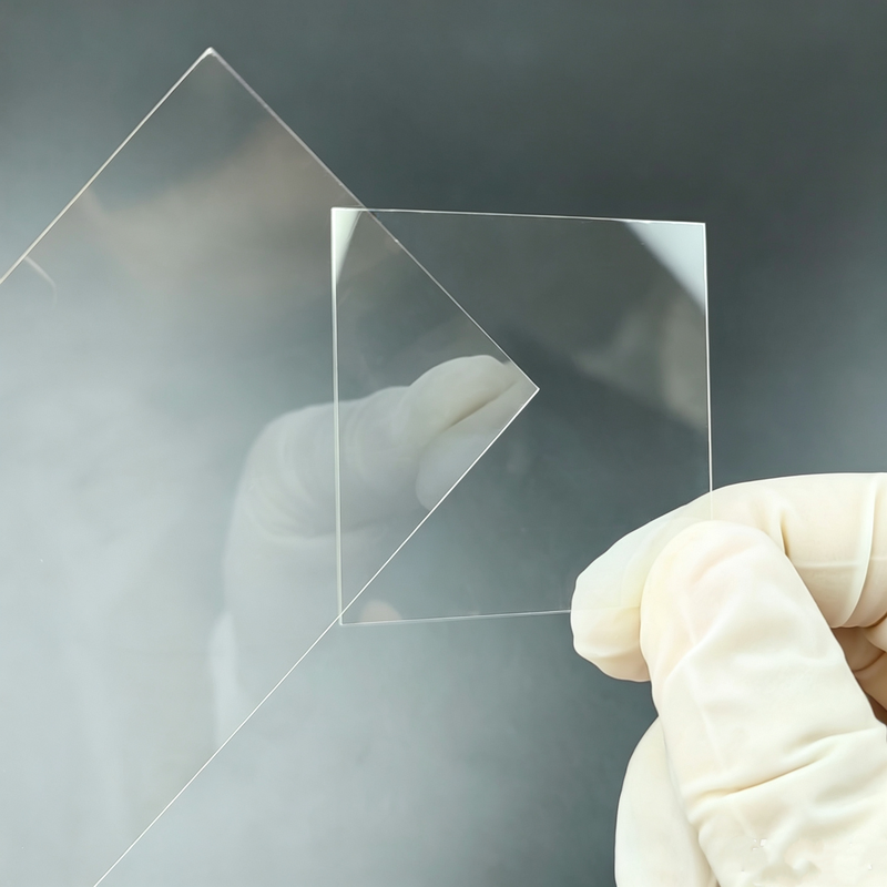
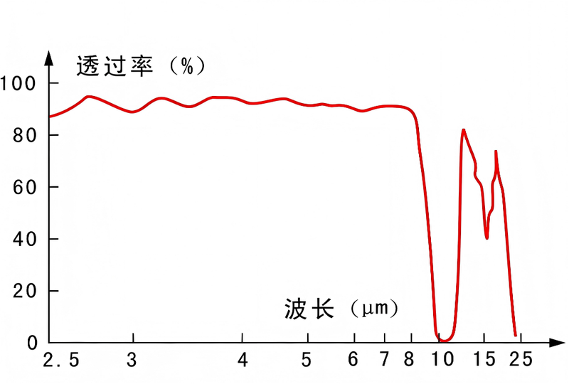
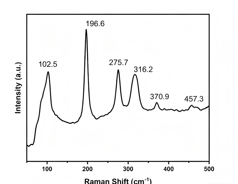
Synthetic Fluorophlogopite Mica KMg3(AlSi3O10)F2,Melts1375℃/Long-Term up to1100℃,Colorless Transparent,Strong Acid-Alkali Inert,Stable/Pure/Complete Structure/Flat Cleavage,Easily Split Thin.
 Save to Favorites
Overview
Specifications
| Parameter | Value |
|---|---|
| Fluoromica Substrate - Dimensions | 5 mm × 5 mm |
| Fluoromica Substrate - Dimensions | 10 mm × 10 mm |
| Fluoromica Substrate - Dimensions | 20 mm × 20 mm |
| Fluoromica Substrate - Dimensions | 50 mm × 50 mm |
| Fluoromica Substrate - Dimensions | 50.8mm |
| Fluoromica Substrate - Thickness | 0.2mm |
| Fluorophlogopite Mica Substrate - Main Surface Crystal Orientation | <001> |
| Fluorophlogopite Mica Substrate - Surface Condition | Double-Side Polished |
| Fluoromica Substrate - Roughness | <0.2nm |
| Density | 2.78 ~ 2.85 ×10³ Kg/m³ |
| Bulk Resistivity | 10¹⁵ ~ 10¹⁶ Ω·cm |
| Electrical Breakdown Strength (Dielectric Strength) | 185 ~ 238 kV/mm |
| Melting Point | 1375±5 ℃ |
| Maximum Use Temperature | 1100 ℃ |
| Thermogravimetric Weight Loss (40 ~ 1180℃) | 0.85% |
| Specific Heat Capacity | 836 J/kg·K |
| Linear Thermal Expansion Coefficient | (∥)10 ~ 12 ×10⁻⁶/K; (⊥)15 ~ 25 ×10⁻⁶/K |
| Thermal Conductivity | (∥)3.75 W/m·K; (⊥)0.55 W/m·K |
| Optical-Axis Angle | 8° ~ 14° |
| Refractive Index | nₚ:1.513 ~ 1.544; nₘ:1.539 ~ 1.564; n₉:1.540 ~ 1.566 |
| Hardness | Mohs Hardness 3~3.4; Microhardness Hv0.2: 1.35 GPa; S: 138~146 |
| Tensile Strength | 150 ~ 200 MPa |
| Compressive Strength | 400 ~ 520 MPa |
Applications
Key Features
Datasheet
Please provide your email to download the datasheet.
Invalid email format. Please try again.
Supplier Information
Related Products
-
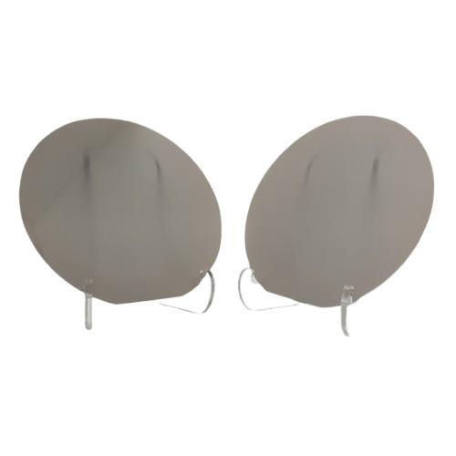 Lithium Tantalate Wafer LT
Optical Crystals
Jmwafer
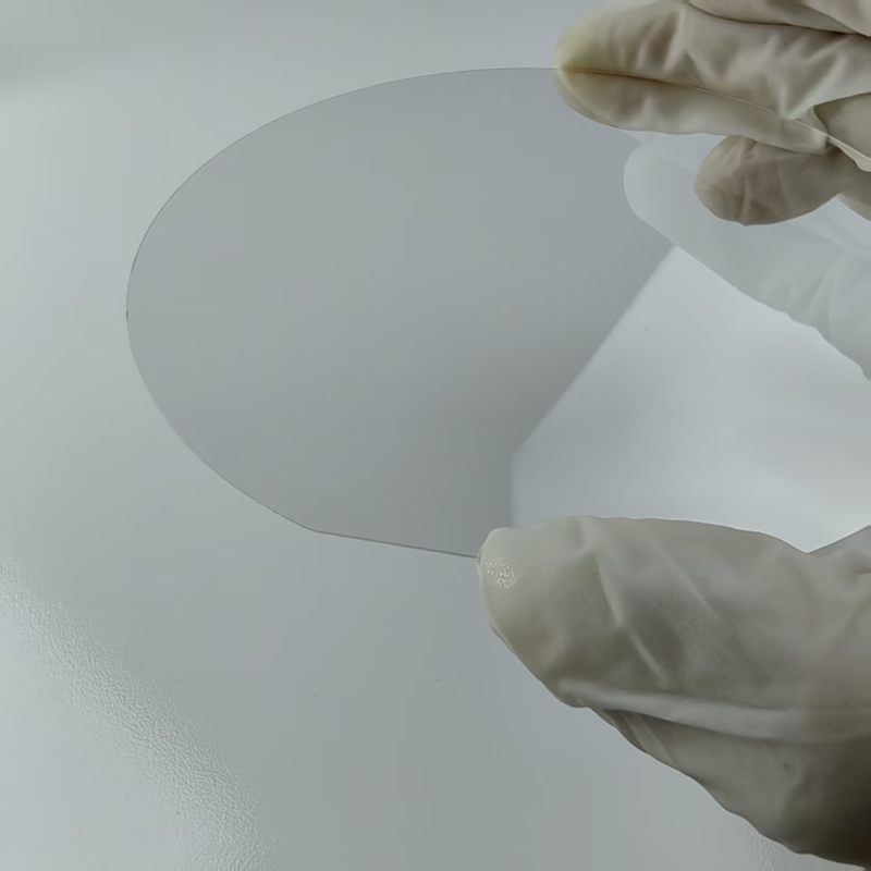
Diameter [Lithium Tantalate Single-Crystal Substrate LiTaO3/LT (2~6 Inches)]: 2 inch - 50.8mm Diameter [Lithium Tantalate Single-Crystal Substrate LiTaO3/LT (2~6 Inches)]: 3 inch - 76.2mm Diameter [Lithium Tantalate Single-Crystal Substrate LiTaO3/LT (2~6 Inches)]: 4 inch - 100mm
LiTaO₃ Usually Colorless/Pale Yellow,Trigonal Distorted-Perovskite Structure,Excellent Electro-Optic,Piezoelectric/Pyroelectric Properties.
-
 Lithium Niobate Wafer LN
Optical Crystals
Jmwafer
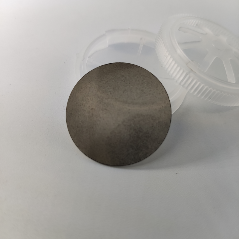
Diameter [Lithium Niobate Single-Crystal Substrate LiNbO3/LN (2~6 Inches)]: 2 inch - 50.8mm Diameter [Lithium Niobate Single-Crystal Substrate LiNbO3/LN (2~6 Inches)]: 3 inch - 76.2mm Diameter [Lithium Niobate Single-Crystal Substrate LiNbO3/LN (2~6 Inches)]: 4 inch - 100mm
LiNbO₃ Trigonal,Good Symmetry/Structural Stability,Piezoelectric,Ferroelectric,Photoelectric,Acousto-Optic/Nonlinear Properties,Curie up to1140℃,High Mechanical Quality/Chemical Stability.
-
 Polycrystalline Diamond
Optical Crystals
Jmwafer
Polycrystalline Diamond - Dimensions: 10 mm × 10 mm Polycrystalline Diamond - Dimensions: 1 inch - 25.4mm Polycrystalline Diamond - Dimensions: 2 inch - 50.8mm
Diamond:Tetrahedrally Packed Carbon,Extremely Hard,Excellent Thermal Conductivity/Broad Optical Transparency,Hardest Known Natural Material,Also Synthesized at High Pressure/Temperature.
-
 Single-Crystal Diamond
Optical Crystals
Jmwafer
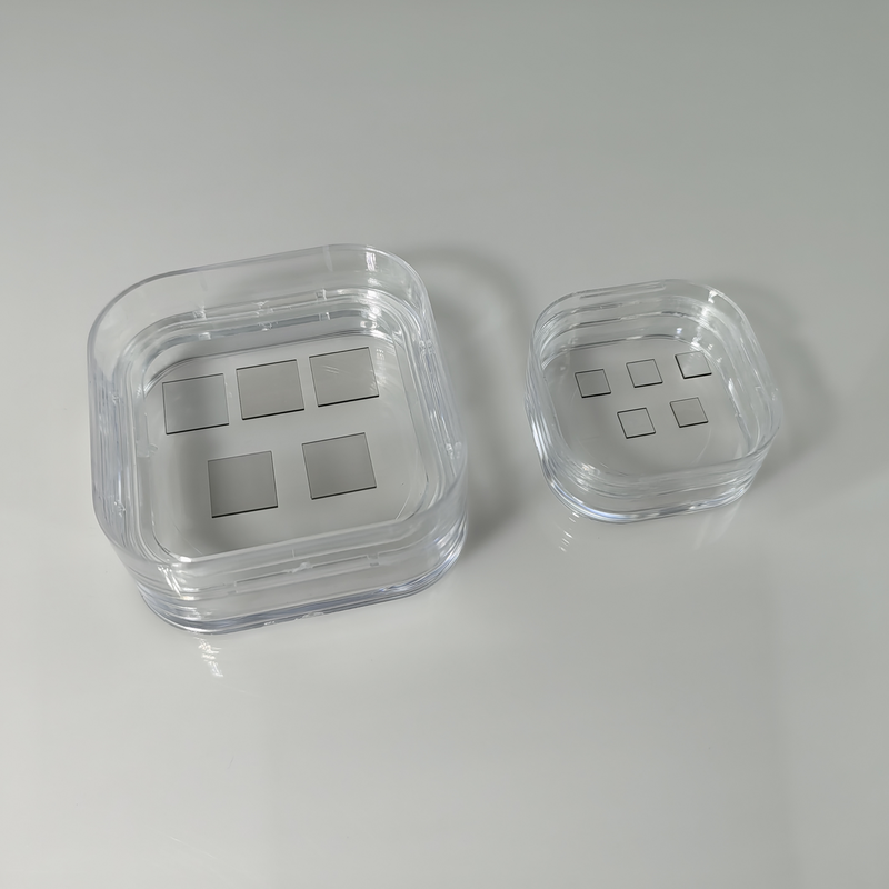
Single-Crystal Diamond - Diameter: 5 mm × 5 mm Single-Crystal Diamond - Diameter: 10 mm × 10 mm Single-Crystal Diamond - Diameter: 20 mm × 20 mm
Diamond:Tetrahedrally Packed Carbon,Extremely Hard,Excellent Thermal Conductivity/Broad Optical Transparency,Hardest Known Natural Material,Also Synthesized at High Pressure/Temperature.
Related Articles
Founded in 2019, Jilin JC Ultrafast Equipment Co., Ltd. is a high-tech enterprise incubated by the Ultrafast Optoelectronics Center of Jilin University. Our R&D team owns 15 years of profound experience in femtosecond laser micro-nano fabrication.
VCSEL, short for Vertical Cavity Surface Emitting Laser, is a widely used semiconductor laser component in modern optoelectronics. Unlike traditional edge-emitting lasers, VCSEL emits laser light vertically from its chip surface. Thanks to its low power consumption, stable beam quality, low cost, and easy integration, it has become the core light source for 3D sensing, wearable devices, and high-speed optical communication.
Driven by the rapid upgrading of intelligent vehicles, optoelectronic sensing technologies represented by laser sensing and infrared thermal imaging have become core pillars for high-level autonomous driving and smart cockpit iteration. Leveraging automotive-grade optoelectronic R&D advantages, Pilot Technology Group launches the VITAL intelligent vehicle solution. By integrating high-power VCSEL laser chips and vehicle infrared night-vision thermal imagers, the system comprehensively enhances vehicle environmental perception and realizes safer, smarter and more comfortable driving experiences.
The MSL‑T series water‑cooled continuous‑wave single‑longitudinal‑mode lasers from Changchun New Industries Optoelectronics (CNI) deliver key research wavelengths including 369 nm, 405 nm and 770 nm.
Loading...
Name
Phone
Organization
Use Case

Database Platform