
Silicon oxide
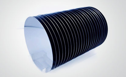
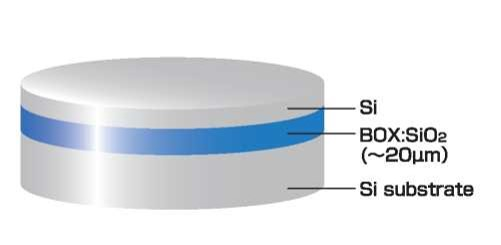
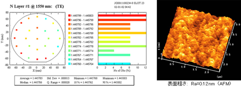
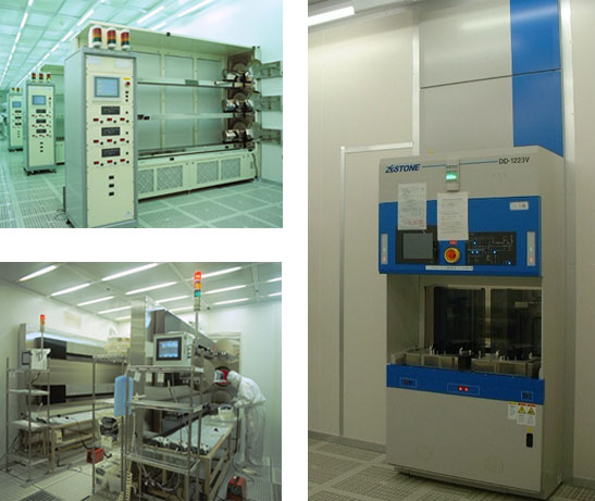
Thermal oxidation thick membrane has the highest market share in the world with superior surface cleanness and abating quality.
 Save to Favorites
Overview
Specifications
| Parameter | Value |
|---|---|
| Menmity | 20um ± 5% (max. thickness) |
| It's all about sex. | ±0.5 % |
| It's all about sex. | ±0.5 % |
| Refractive rate (@1550nm) [@1550nm;@1550nm)] | 1.4458±0.0001 |
| 4nch-clinical thickness | 525um 1mm |
| 4nch - Heat oxide film thickness | 15um、20um |
| 6incch-clinic thickness | 625um 675um 1mm |
| 6nch - Heat oxide film thickness | 15um、20um |
| 8inch-clinical thickness | 725 um |
| 8inch - Heat oxide film thickness | 15um、20um |
| 12inch-clinical thickness | 775 um |
| 12inch - Heat oxide film thickness | 15 um |
Applications
Datasheet
Please provide your email to download the datasheet.
Invalid email format. Please try again.
Supplier Information
Related Products
-
 Sapphire A-R-M Special Crystal-Orientation Substrate
Optical Material
Jmwafer
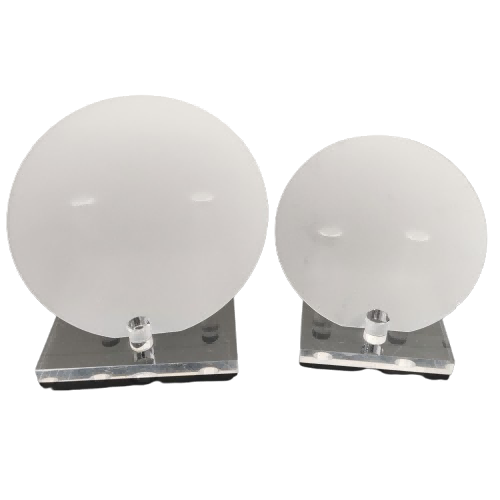
A-M-R Orientation Single-Crystal Sapphire Substrate (2~6 Inches) - Material Composition: >99.99%,High Purity, Mono-crystalline Al2O3 (KY) Sapphire A/M/R-Plane Single-Crystal Substrate (2~6 Inches) - End-Face Crystal Orientation [Diameter: 50.8mm]: A-plane (11-20) ± 0.1° Sapphire A/M/R-Plane Single-Crystal Substrate (2~6 Inches) - End-Face Crystal Orientation [Diameter: 100mm]: A-plane (11-20) ± 0.1°
α-Al2O3 Hexagonal Lattice,Chemically Stable/Water-Insoluble/Strong Acid-Alkali Resistant,Mohs9,Melts2050℃/Boils3500℃,Operating up to1900℃,Good Transmission/Thermal Conduction/Insulation/Mechanics,Wear/Scratch Resistance.
-
 N-Type Silicon Carbide Epitaxy
Optical Material
Jmwafer
N-Type Silicon Carbide Epitaxial Substrate (2~8 Inches) - Substrate Diameter: 2 inch - 50.8mm N-Type Silicon Carbide Epitaxial Substrate (2~8 Inches) - Substrate Diameter: 4 inch - 100mm N-Type Silicon Carbide Epitaxial Substrate (2~8 Inches) - Substrate Diameter: 6 inch - 150mm
N-Type SiC Epitaxy Grows N-Doped Layer on SiC,High Electron Mobility/Thermal Conductivity/Breakdown Field.
-
 Silicon-Based GaN Epitaxial Template
Optical Material
Jmwafer
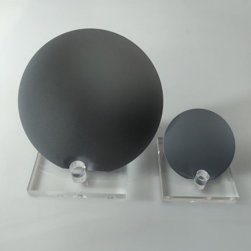
Silicon-Based GaN Epitaxial Template Substrate (2~8 Inches) - Substrate Diameter: 50.8mm Silicon-Based GaN Epitaxial Template Substrate (2~8 Inches) - Substrate Diameter: 100mm Silicon-Based GaN Epitaxial Template Substrate (2~8 Inches) - Substrate Diameter: 150mm
GaN-on-Si Epitaxy Grows GaN Films on Silicon,Combining GaN Performance with Low-Cost Silicon.
-
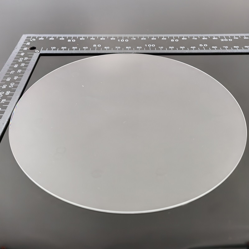 High-Borosilicate Glass BF33
Optical Material
Jmwafer
High-Borosilicate Glass - Material: BF33 High-Borosilicate Glass - Diameter: 50.8mm High-Borosilicate Glass - Diameter: 100mm
BF33 Special Borosilicate Glass with Low Expansion,Heat Resistance,Chemical Stability and Excellent Transmission.
-
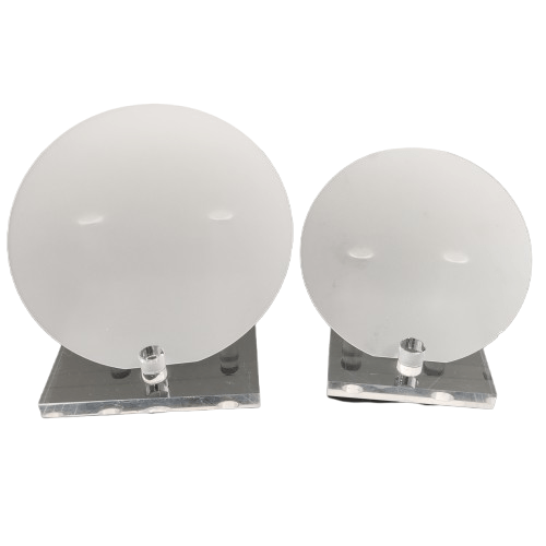 Sapphire-Based GaN Epitaxial Template
Optical Material
Jmwafer
Sapphire-Based GaN Epitaxial Template Substrate (2~8 Inches) - Substrate Diameter: 50.8mm Sapphire-Based GaN Epitaxial Template Substrate (2~8 Inches) - Substrate Diameter: 100mm Sapphire-Based GaN Epitaxial Template Substrate (2~8 Inches) - Substrate Diameter: 150mm
GaN-on-Sapphire Epitaxial Template Grows GaN Film on Al₂O₃,Common Substrate for Heat/Chemical Stability/Cost Advantages.
Related Articles
An infrared transmitter (IR transmitter) is a basic electronic component that sends invisible infrared light signals for short-range wireless control. It is widely used in daily electronics, smart home devices, and industrial equipment due to its low cost, low power consumption, and stable performance.
In photonics and laser technology, devices that manipulate optical signals via the electro-optic effect form the backbone of precision optical systems. Electro-optic phase modulators and electro-optic deflectors are two prominent examples of this device category. As a critical hardware solution for high-speed, high-accuracy laser beam direction control, electro-optic deflectors are widely deployed across industrial and research settings. Below is a detailed overview of their core structure, key performance drivers, and primary use cases.
Founded in 2019, Jilin JC Ultrafast Equipment Co., Ltd. is a high-tech enterprise incubated by the Ultrafast Optoelectronics Center of Jilin University. Our R&D team owns 15 years of profound experience in femtosecond laser micro-nano fabrication.
Wuhan Optical Valley Interlink Technology Co., Ltd. was founded in 2013 by a technical team from Huazhong University of Science and Technology.
Loading...
Name
Phone
Organization
Use Case

Database Platform