
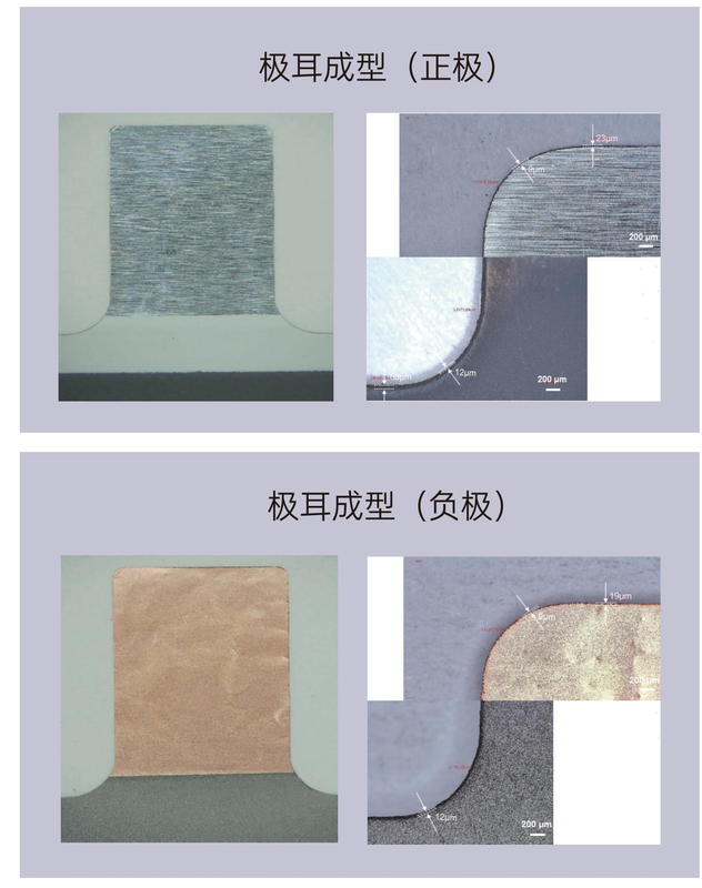
Battery tab forming
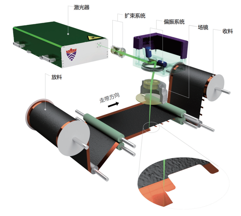
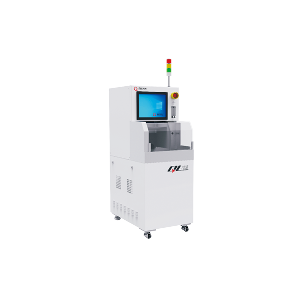
The precision laser forming and cutting system processes lithium-battery electrodes and tabs. Advanced laser processing forms tabs precisely with consistent dimensions and no burrs, and cuts electrodes rapidly and cleanly without dust, avoiding microscopic short-circuit risks from mechanical methods. It also supports continuous online electrode forming for complex shapes and precise dimensions. Noncontact, stress-free processing has no tool wear and integrates into automated lines, improving battery safety, reliability, production flexibility and efficiency.
 Save to Favorites
Overview
Specifications
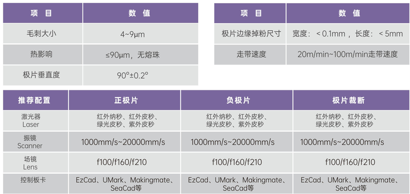
| Parameter | Value |
|---|---|
| 毛刺大小 | 4~9μm |
| 热影响 | ≤90μm, without melt beads |
| 极片垂直度 | 90°±0.2° |
| 极片边缘掉粉尺寸-宽度 | <0.1mm |
| 极片边缘掉粉尺寸-长度 | <5mm |
| 走带速度 | 20m/min~100m/min |
Applications
Key Features
Datasheet
Please provide your email to download the datasheet.
Invalid email format. Please try again.
Supplier Information
Related Products
-
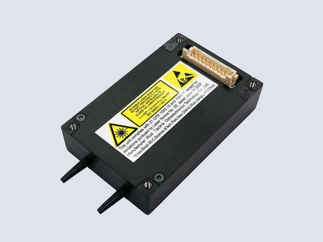 Mini EDFA Series
Semiconductor Packaging Equipment
Taclink
size: 35 mm x18 mm x5.5 mm, Smaller Output Power: >4dBm Power Consumption: <2w
Mini EDFA series, its main features are small size and low power.
-
 Single-axis precision dicing machine (semi-automatic)
Semiconductor Packaging Equipment
Qhlaser
Stage format: 310 mm × 310 mm X-axis working stroke: 0-600 mm Y1, Y2 axis working stroke: 0-500mm
● Wafer cutting equipment using high-precision bidirectional silent air spindle:; ● Cutting area: 4 inch, 6 inch wafers;; ● High precision: for resin substrates with irregular expansion and contraction, high-precision processing is possible through cutting line calibration at multiple points;; ● Simple and convenient operation: 17-inch touch screen;; ● Automatic blade mark calibration function: automatically measures the offset of the cutting street and the width of the cutting mark, managing processing quality;; ● Blade breakage detection function: blade breakage detection during cutting.; ● 4/6 inch IC, wafer cutting; ● Silicon, quartz, aluminum oxide, iron oxide, gallium arsenide, sapphire, glass, etc.
-
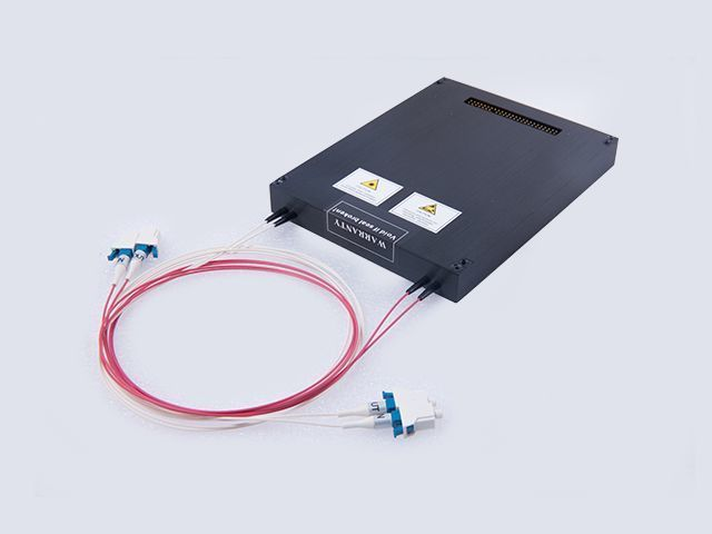 Normal EDFA Series (EDFA-BA,PA,LA)
Semiconductor Packaging Equipment
Taclink
Power: High power and High gain Gain ripple [typ. condition]: <1.0dB typ. condition NF [for typ. C Condition]: <6.0dB for typ. C Condition
Normal-type EDFA, including single-wave, multi-wave, pure optical, and powered EDFA, with dimensions above 90*70*15mm, can achieve higher gain and larger power output.
-
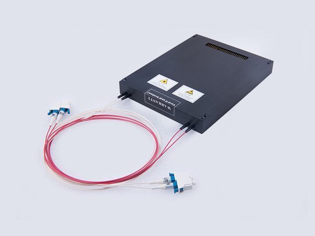 Normal EDFA Series (EDFA-VGA)
Semiconductor Packaging Equipment
Taclink
Variable Gain Range: >10dB Power: >18dBm Gain ripple [typ. condition]: <1.0dB typ. Condition
Normal-type EDFA, including single-wave, multi-wave, pure optical, and powered EDFA, with dimensions above 90*70*15mm, can achieve higher gain and larger power output.
Related Articles
VCSEL, short for Vertical Cavity Surface Emitting Laser, is a widely used semiconductor laser component in modern optoelectronics. Unlike traditional edge-emitting lasers, VCSEL emits laser light vertically from its chip surface. Thanks to its low power consumption, stable beam quality, low cost, and easy integration, it has become the core light source for 3D sensing, wearable devices, and high-speed optical communication.
Medical disposable‑device manufacturers have long demanded high‑performance interconnect accessories for single‑use equipment. The newly‑launched REDEL‑P disposable‑connector family addresses this requirement and delivers premium‑grade electrical connections for varied one‑time‑use medical instruments.
On January 21, 2026, SPIE Photonics West, one of the world’s leading photonics events, was held in San Francisco, USA. RaySea presented its latest self‑developed VCSEL achievements at this prestigious exhibition. Dr. Lai, the company’s senior R&D representative, delivered a technical speech during the dedicated VCSEL session. His presentation covered cutting‑edge progress of in‑house multi‑junction VCSEL solutions built for automotive lidar and embodied‑intelligence robots, drawing strong attention from the global photonics community.
Shandong Optochip specializes in independent R&D of industrial-grade optical chips for optical communication and fiber sensing. Our business includes overseas chip tape-out, domestic precision device packaging
Loading...
Name
Phone
Organization
Use Case

Database Platform