
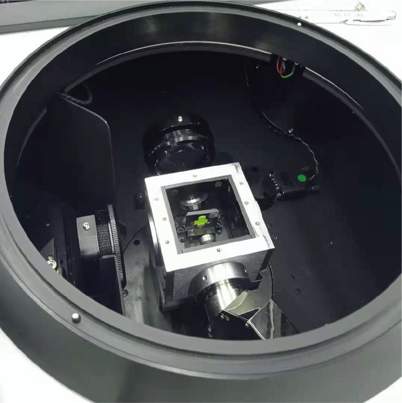
Ce:YAG
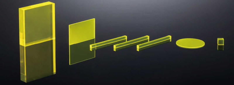
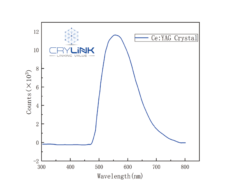
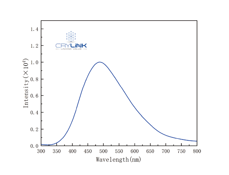
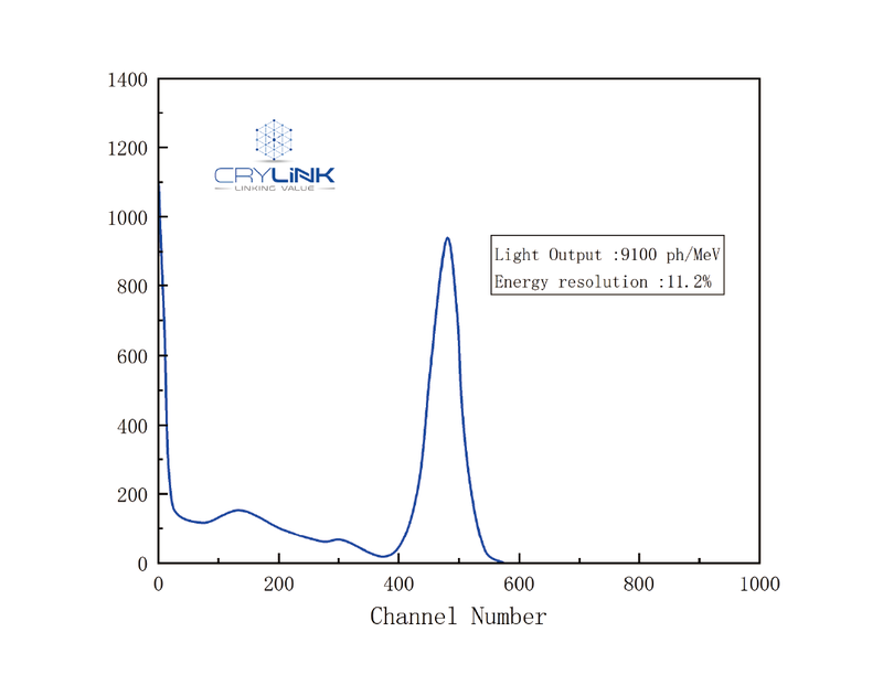
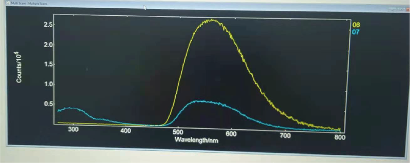
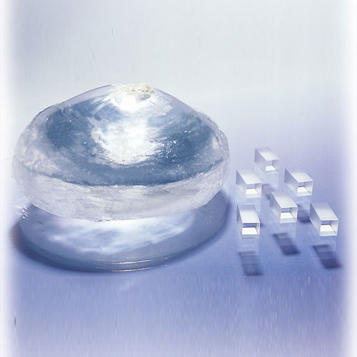
Ce:YAG single crystal is a fast-decay scintillation material with good overall performance. It offers high light output (20000 photons/MeV), fast luminescence decay (~70ns), and excellent thermal and mechanical properties. Its peak emission wavelength (540nm) matches the sensitive spectral ranges of common photomultiplier tubes (PMT) and silicon photodiodes (PD). Its light pulses distinguish γ rays from α particles. Ce:YAG is suitable for detecting charged particles such as α particles, electrons and β rays. Its good mechanical properties make it possible to prepare films less than 30um thick. Ce:YAG scintillation detectors are widely used in electron microscopes, β-ray and X-ray counting, and electron and X-ray imaging screens. Ce:YAG scintillation crystal — a fast-decay scintillation material for white LEDs. Ce:YAG single crystal has distinct absorption peaks at 340nm and 460nm, characteristic of Ce³⁺. The InGaN blue chips used in commercial white LEDs emit at 460nm. The broad absorption band of Ce:YAG single crystal centered at 460nm enables it to absorb blue light from the chip effectively. Combining this blue light with the yellow light emitted by the Ce:YAG wafer produces white light. Ce:YAG also has good thermal stability, which is particularly important in manufacturing high-power white LED devices. As the Ce:YAG wafer becomes thicker, the luminous efficiency of white LED devices packaged with a blue chip and Ce:YAG wafer gradually increases, while their color temperature and color rendering index gradually decrease. With increasing wafer thickness, the relative amount of Ce³⁺ increases. More blue light is absorbed and more yellow light is emitted, shifting the wafer's emission from blue to white and then to yellow.
 Save to Favorites
Overview
Specifications
| Parameter | Value |
|---|---|
| Chemical formula | Ce:Y₃Al₅O₁₂ |
| Density | 4.55 g/cm₃ |
| Melting point | 1970 ℃ |
| Hardness | 8.5 Mho |
| Hygroscopicity | None |
| Cut | None |
| Coefficient of thermal expansion | 8.5*10⁻⁶ C⁻¹ |
| Wavelength (maximum emission) | 550 nm |
| Wavelength Range | 500-700 nm |
| Attenuation Time | 70 ns |
| Light yield | 9000-14000 Photons/Mev |
| Refractive index (maximum emission) | 1.82 |
| Radiation length | 3.5 cm |
| Energy Resolution | 7.5 % |
| Light emission [% of NaI(Tl)] (for Υ rays) | 35 |
Applications
Key Features
Datasheet
Supplier Information
Related Products
-
 Dia.100mm TeO2 boule
Optical Crystals
Xkpho
Chemical equation: TeO2 Density: 6 g/cm² Melting point: 733 ℃
TeO2 is a kind of acousto-optic material with high quality factor. It has good properties of birefringence and optical rotation with low velocity of propagation along (110) axis.Under the same clear aperture, the acousto-optic device produced by TeO2 crystal has the advantages of the orders of magnitude improvement in resolution, fast response speed, small driving power, high diffraction efficiency, as well as stable and reliable performance. TeO2 crystal is an ideal single crystal material used to produce different kinds of acousto-optic device, such as acousto-optic deflector, modulator, resonator and tunable filter.
-
 LBO
Optical Crystals
Xkpho
Tolerance of cutting angle: △θ≤±0.25°,△φ≤±0.25° Tolerance of dimension: Dimension+/-0.1 mm,L:±0.1mm Flatness [@ 632.8nm]: λ/8 @ 632.8nm
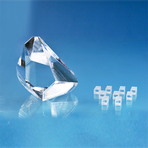
LBO crystals is an excellent nonlinear crystal.For frequency doubling(SHG),tripling(THG) of Nd:YAG,Nd:YLF,Nd:YVO4 lasers, it is one of the most useful nonlinear optical materials in ultraviolet and visible laser applications. LBO has the highest damage threshold in all the commonly-used inorganic NLO crystals. Therefore, it is the best candidate for high average power SHG and other nonlinear optical processes.
-
 TGG
Optical Crystals
Xkpho
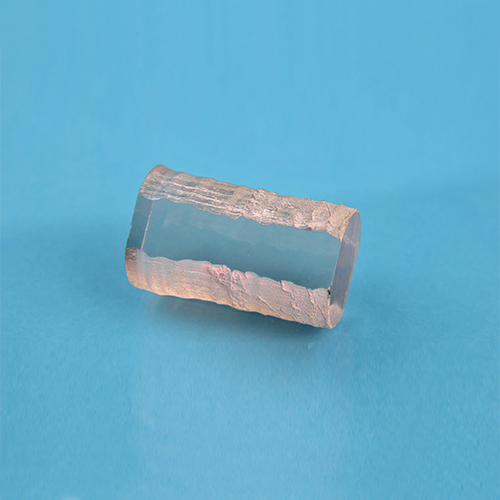
Chemical Formula: Tb₃Ga₅O₁₂ Lattice Parameter a: a=12.355Å Growth Method: Czochralski
TGG is an excellent magneto-optical crystal used in various Faraday devices (Rotator and Isolator) in the range of 400nm-1100nm, excluding 475-500nm.
-
 Ultra thin BBO crystal wafer
Optical Crystals
Xkpho
Crystal Structure: Trigonal,Space Group R3c Lattice Parameter: a=b=12.532Å,c=12.717Å,Z=6 Melting Point: About 1095℃
BBO is a negative uniaxial crystal, with ordinary refractive index (No) larger than extraordinary refractive index (Ne). Both type I and type II phase matching can be reached by angle tuning. The phase matching angles of frequency doubling are shown in Fig. 2. Figure1. Transparency curve of BBO Figure2. SHG tuning curves of BBO The OPO and OPA of BBO are powerful tools for generating a widely tunable coherent radiation from UV to IR. The tuning angles of type I and type II BBO OPO and OPA have been calculated, with the results shown in Fig. 3 and Fig. 4, respectively. Figure 3. Type I OPO tuning curves of BBO Figure 4. Type II OPO tuning curves of BBO 1. OPO pumped at 532 nm An OPO output ranging from 680 nm to 2400 nm with the peak power of 1.6MW and up to 30% energy conversion efficiency was obtained in a 7.2 mm long type I BBO. The input pump energy was 40 mJ at 532 nm with pulse-width 75ps. With a longer crystal, higher conversion efficiency is expected. 2. OPO and OPA pumped at 355 nm In the case of Nd:YAG pumping, BBO's OPOs can generate more than 100mJ, with wavelength tunable from 400nm to 2000nm. Using XKPHO's BBO crystal, the OPO system covers a tuning range from 400nm to 3100nm which guarantees a maximum of 30% and more than 18% conversion efficiency, over the wavelength range from 430nm to 2000nm. Type II BBO can be used to decrease linewidth near the degenerate points. A linewidth as narrow as 0.05 nm and usable conversion efficiency of 12% were obtained. However, a longer (> 15mm) BBO should normally be used to decrease the oscillation threshold when employing the type II phase-matching scheme. Pumping with a picosecond Nd:YAG at 355 nm, a narrow-band (< 0.3 nm), high energy (> 200μJ) and wide tunable (400 nm to 2000 nm) pulse has been produced by BBO's OPAs. This OPA can reach as high as more than 50% conversion efficiency, and therefore is superior to common Dye lasers in many respects, including efficiency, tunable range, maintenance, and easiness in design and operation. Furthermore, coherent radiation from 205 nm to 3500 nm can be also generated by BBO's OPO or OPA plus a BBO for SHG. 3. Others A tunable OPO with signal wavelengths between 422nm and 477nm has been generated by angle tuning in a type ⅠBBO crystal pumped with a XeCl excimer laser at 308 nm. And a BBO's OPO pumped by the fourth harmonic of a Nd:YAG laser (at 266 nm) has been observed to cover the whole range of output wavelengths 330 nm - 1370 nm. When pumped by a 1mJ, 80 fs Dye laser at 615 nm, the OPA with two BBO crystals yields more than 50μJ (maximum 130 μJ), < 200 fs ultrashort pulse, over 800 nm - 2000 nm.
-
 BBO Crystal Basic characteristics
Optical Crystals
Iloptik
Basic Properties - Crystal Structure [Negative Uniaxial Crystal]: Trigonal Crystal System Basic Properties - Unit Cell Parameters [Room temperature]: a=b=12.532 Å,c=12.717 Å,Z=6 Basic Properties-Melting Point: 1095±5 ℃
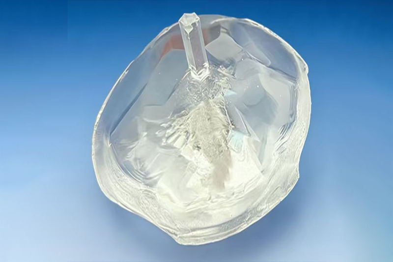
BBO, β-barium borate crystal (β-Barium Borate Crystal), is an important nonlinear optical crystal widely used in laser technology and one of the most established nonlinear optical crystals for the ultraviolet band.
Related Articles
icrolight is a high-tech enterprise specializing in the R&D, manufacturing and sales of active and passive photonic devices for microwave photonics, LiDAR ranging, gas sensing, fiber optics and photomedicine.
Against the evolving demands for military‑grade hardware, rail transit equipment and heavy‑duty machinery that run under high‑shock vibrating conditions, anti‑loose connectors serve as indispensable hardware for stable power delivery and high‑speed signal transmission.
For low-frequency RF, electromagnetic testing and power combining systems, conventional resistive power dividers bring high insertion loss, while standard directional couplers cannot provide equal-amplitude signals with 180° phase shift. They fail differential circuits, balanced amplifiers and signal cancellation systems.
For pulsed laser and full-spectrum optical testing, photodiodes and thermopiles have inherent drawbacks. Photodiodes show weak response in infrared band, while thermopiles feature slow response and cannot capture nanosecond narrow pulses.
Loading...
Name
Phone
Organization
Use Case

Database Platform