
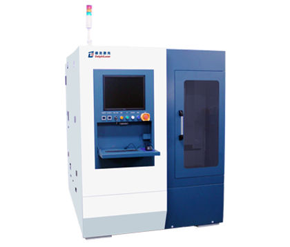
Wafer Laser Stress-Induced Cutting Equipment
Stress-induced cutting of Mini LED wafers.
 Save to Favorites
Overview
Specifications
| Parameter | Value |
|---|---|
| Laser Type | Diode-Pumped Picosecond Laser |
| Laser Power | ≥1W |
| Cooling method | Closed-loop circulating water cooling |
| X Axis - Travel | 360mm |
| X-Axis Resolution | 0.1um |
| Y Axis - Travel | 300mm |
| Y-Axis Resolution | 0.1um |
| Z Axis - Travel | 15mm |
| Z-Axis Resolution | 1um |
| θ Axis - Travel | ±60° |
| θ-Axis Resolution | 0.0001° |
| Dicing speed | ≤1000mm/s |
| 4-Inch Processing Capacity [@10*30mil(4 inches )] | 15pcs/h@10*30mil(4 inches ) |
| Dicing dimensions [Can Be Upgraded 6 inch] | 2 inch 、4 inch ( Can Be Upgraded 6 inch ) |
| Dual-Focus Function | Optional |
Applications
Key Features
Datasheet
Please provide your email to download the datasheet.
Invalid email format. Please try again.
Supplier Information
Related Products
-
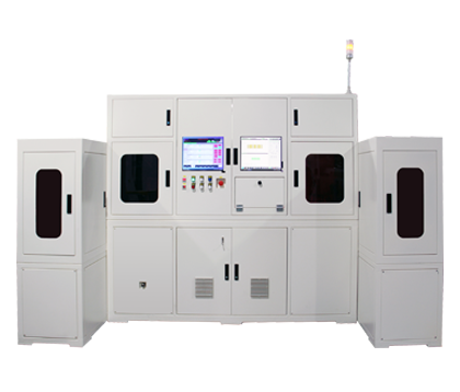 ATM50 Fully Automatic Laser Coding Equipment (On boat)
Laser Processing Equipment
Delphilaser
Slot Type Magazine-Product Length: 100-320mm Slot Type Magazine-Product Width: 45-180mm Slot Type Magazine-Handler slot magazine Capacity [Calculated for 180 x320mm]: 2 (Calculated for 180 x320mm)
This equipment uses a laser to mark individual devices on a BOAT with customized QR codes, characters, LOGO and other patterns.
-
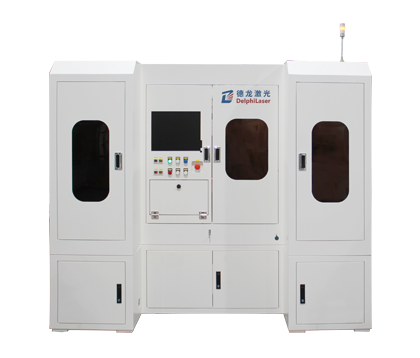 ATM90 Fully Automatic Laser Marking Machine (MiniQFN)
Laser Processing Equipment
Delphilaser
Workpiece Dimensions: Max 280 x 100mm;Min 150 x 60mm Print Content: 2D, Logo, PIN, Text Printing Specifications-Depth Control: ±6um
Fully automatic laser marking of packaged semiconductor Mini QFN products.
-
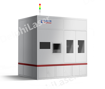 BUSBAR Laser Cleaning Equipment
Laser Processing Equipment
Delphilaser
Equipment Dimensions: L2.5m×W2.0m×H2.7m Terminal Cleaning Area: 160 mm × 160 mm
BUSBAR laser cleaning for new-energy battery modules.
-
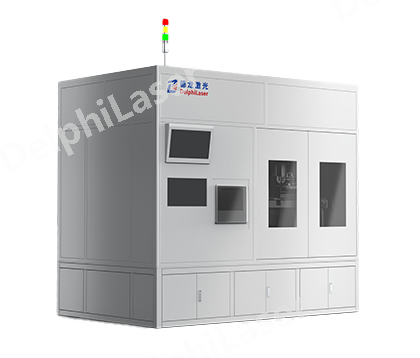 BUSBAR Laser Welding Equipment
Laser Processing Equipment
Delphilaser
Equipment Dimensions: L2.8m×W2.0m×H2.7m Equipment Operating Efficiency [Calculated by Battery Cell Count]: ≥10PPM(Calculated by Battery Cell Count) Compatible Battery Modules: L1200mm×W200mm×H240mm
BUSBAR laser welding for new-energy battery modules.
-
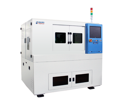 DPC Ceramic Substrate Rapid Drilling Equipment RPS10
Laser Processing Equipment
Delphilaser
Equipment Type: Single Head Working area: 250mm×250mm/450mm×450mm(customizable) Positioning accuracy: ±3μm
Depending on thickness, material and processing-quality requirements, drilling or cutting equipment can be selected for drilling, cutting or punching most DPC ceramics, including alumina (Al2O3), aluminum nitride (AlN) and zirconia (ZrO2).
Related Articles
As a core precision optical component for wavelength screening, frequency locking and spectral demodulation, optical etalons are widely used in high-end scientific research and precision laser equipment.
As a vital emerging sector of modern three-dimensional spatial economy, the low-altitude economy has become a new global growth driver. It covers a wide range of commercial scenarios, including UAV navigation and obstacle avoidance, precise airspace management, aerial mapping, low-altitude logistics distribution, security monitoring and emergency disaster rescue. Nevertheless, frequent extreme weather, complex terrain obstacles and increasingly dense low-altitude flight activities pose severe challenges to the safety and stability of low-altitude aircraft operations.
Laser pump sources are the core energy input component of solid-state lasers and laser amplifiers, and their performance directly determines the output power, beam quality and service life of the entire laser system. In scenarios such as industrial processing, scientific research experiments and high-end equipment, improper pump source selection will not only result in substandard system performance, but also bring a series of problems such as rapid device degradation and high operation and maintenance costs. This article sorts out the core selection logic and key pitfalls of pump source procurement, and provides selection references based on mature, mass-produced high-reliability products to help purchasers efficiently screen suitable products.
Shandong Haucore Optoelectronics Co., Ltd. introduces the HGLD‑792‑COS‑D‑10WB semiconductor laser within its COS series. Delivering an output power of 10 W at a central wavelength of 792 nm, this device adopts gold‑tin bonding COS packaging. Featuring high reliability and long service life, it serves as a preferred pump source for solid‑state lasers and is widely deployed in industrial processing, laser display, medical & aesthetic treatment, scientific research and other fields.
Loading...
Name
Phone
Organization
Use Case

Database Platform