
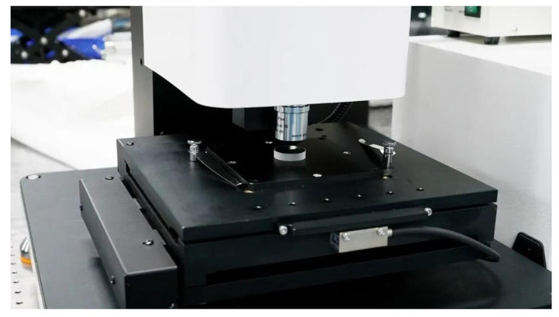
White Light Interferometer
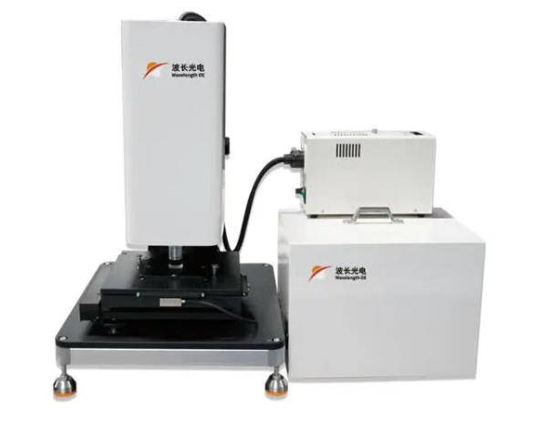
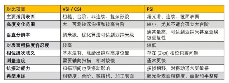
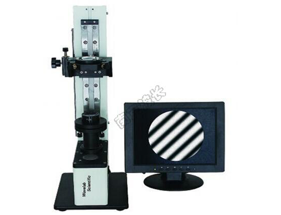
The surface roughness, step height, and film thickness inspection of semiconductor wafers, precision optical components, and thin-film coatings directly determines the yield of finished products. Traditional probe measurement easily scratches the workpiece, and ordinary optical equipment has insufficient precision. How can one balance non-destructive, nanometer high-precision, and efficient mass-production inspection? Wavelength Opto-Electronic's brand-new industrial-grade white light interferometer is equipped with dual interference measurement modes, using a non-contact inspection solution to connect the entire scenario from laboratory R&D to industrial production line quality inspection. Different from equipment with a single measurement mode, this instrument integrates dual-algorithm modes of Vertical Scanning Interferometry (VSI) + Phase Shifting Interferometry (PSI), and one device satisfies two types of measurement needs: PSI phase-shifting interferometry: specialized in nanometer-level tiny heights and ultra-thin films, with extreme microscopic resolution; VSI vertical scanning interferometry: suitable for measuring workpieces with large height differences and large steps, with sufficient range and no segmentation; Paired with a 450-700nm short-coherence white light source, it can effectively suppress multi-reflection stray light and has strong anti-interference ability. Multi-layer coatings and weakly reflective optical components can also output stable and clear interference signals, and measurement results are true and reliable.
 Save to Favorites
Overview
Specifications
| Parameter | Value |
|---|---|
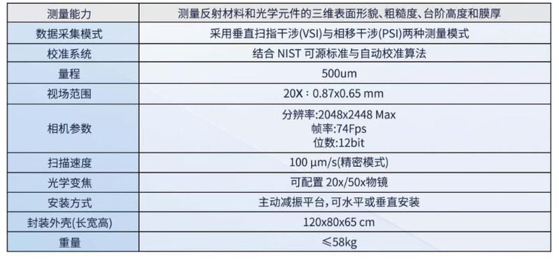
| Measurement capability | Measurement of the 3D surface topography, roughness, step height, and film thickness of reflective materials and optical components |
| Data acquisition mode | Adopts two measurement modes: Vertical Scanning Interferometry (VSI) and Phase Shifting Interferometry (PSI) |
| Calibration system | Combines NIST traceable standards with automatic calibration algorithms |
| Range | 500 um |
| Field of view [20X] | 20X:0.87x0.65 mm |
| Camera parameters - resolution | 2048x2448 Max |
| Camera parameters - frame rate | 74Fps |
| Camera parameters - bit depth | 12 bit |
| Scanning speed [precision mode] | 100 μm/s (precision mode) |
| Optical zoom [configurable] | Configurable 20x/50x objective |
| Installation Method | Active vibration isolation platform, can be installed horizontally or vertically |
| Enclosure housing (length × width × height) | 120 cm × 80 cm × 65 cm |
| Weight | ≤58 kg |
Applications
Key Features
Datasheet
Please provide your email to download the datasheet.
Invalid email format. Please try again.
Supplier Information
Related Products
-
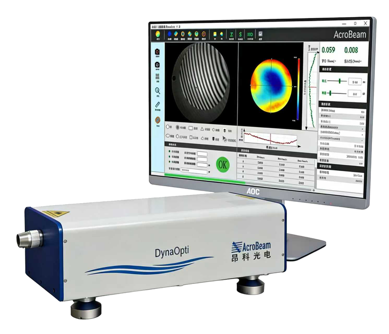 Dyna-Opti instrument
Interferometers
Acrobeam
Instrument Aperture: 9mm, optional amplifier cal. 50-800mm Light: Importing ammonia lasers, 1 = 632.8 mm Camera: 2Kx2K pixel
Dyna-Opti series dynamic interferometer;
-
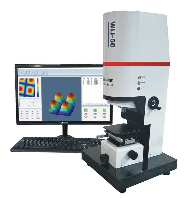 white-light series
Interferometers
Acrobeam
Objective Lens: Infinite interference mirrors 2.5X, 5X, 10X, 20X, 50X (other customable); Infinite intervention lenses 10X (20X optional) Lateral Resolution: 0.4um ~10.2um, related to selected mirrors
The WLI series of white light interferometers are based on white light interferometry;
-
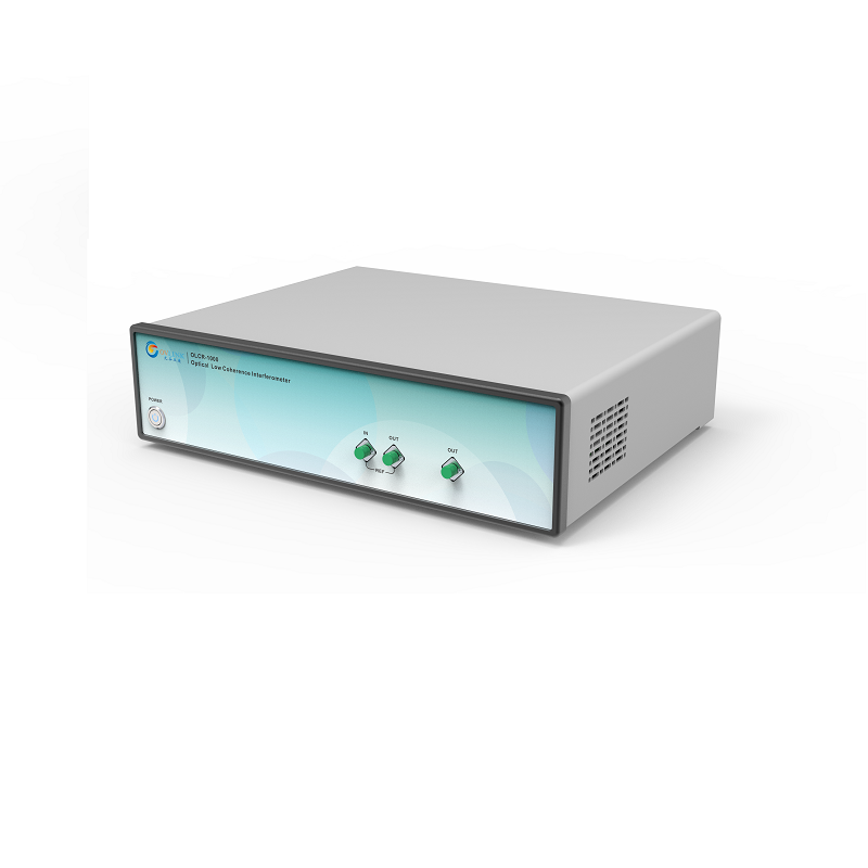 Low-linked light interferometer OCR
Interferometers
Ovlink
Work wavelength: 1310 & 1550nm Measuring length: 50; condition: other measurements can be determined Production Time-consuming single measurement: ^15s
Low-continental light interferometer OLCR-1000 is a distributed fibre-optic reruption detection system based on white light interferometry; detectability recognition that can be used for fibre-optic microfracking, optical devices, photochip reflectors; and have the advantage of being low-cost, high-precision measurement and short time-consuming relative to optical-frequency reflectors. Second-scale measurements; quick-output measurements; micro-level positioning; accurate identification of various reflex events; high-precision backsliding measurements; accurate output of reflection events backsliding; sub-miscale measurements range; greater measurement length customizable
-
 Laser Interferometer
Interferometers
Wave-optics
Related Articles
Wuhan Optical Valley Interlink Technology Co., Ltd. was founded in 2013 by a technical team from Huazhong University of Science and Technology.
Shanghai Connet Laser Technology Co., Ltd. focuses on technological innovation, delivering cutting-edge photonic products & solutions for industrial lasers, LiDAR, fiber optic sensing, coherent telecom, cold atom physics and precision spectroscopy research & mass manufacturing.
Against the evolving demands for military‑grade hardware, rail transit equipment and heavy‑duty machinery that run under high‑shock vibrating conditions, anti‑loose connectors serve as indispensable hardware for stable power delivery and high‑speed signal transmission.
BEIJING JIEPU TREND supplies YAG+Er:YAG+YAG bonded composite slab laser crystals for high‑power solid‑state laser systems. The monolithic slab consists of two undoped YAG end‑cap layers and a central Er‑doped YAG gain segment. The overall dimension is 9 mm×9 mm×9 mm.
Loading...
Name
Phone
Organization
Use Case

Database Platform