


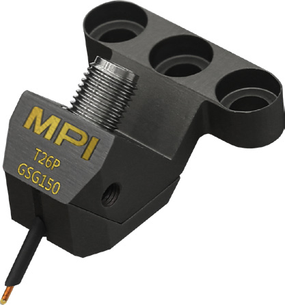
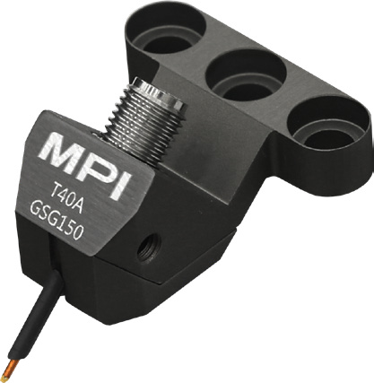
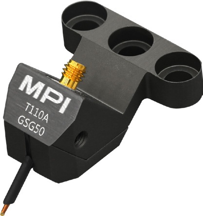

TITAN™ RF Probes
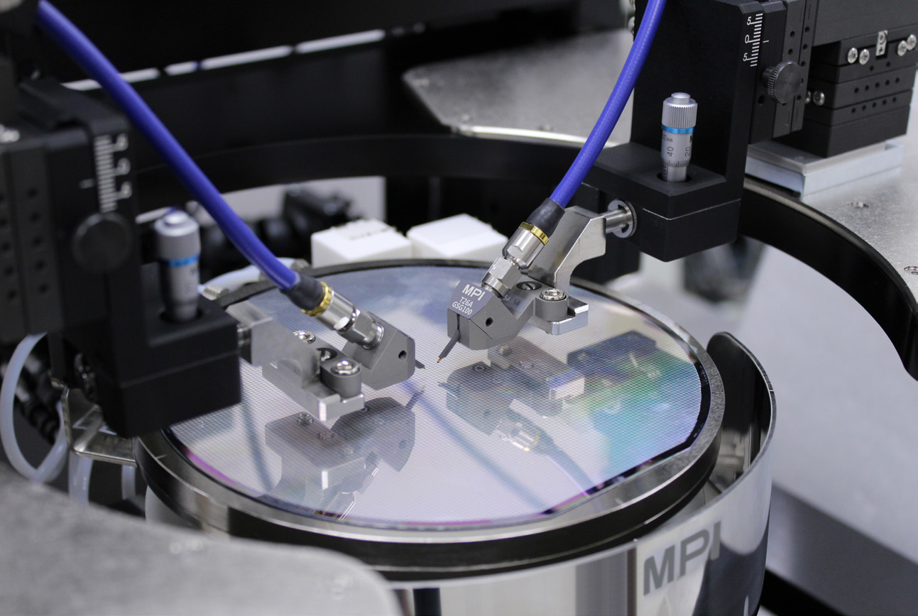
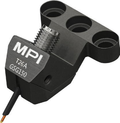
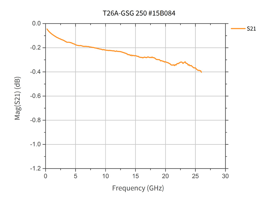
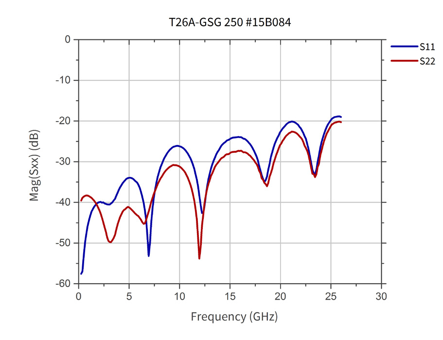
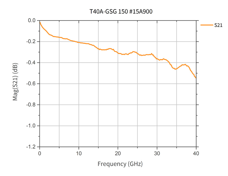
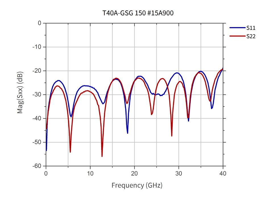
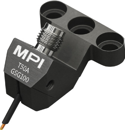
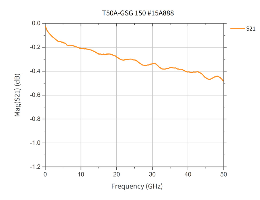
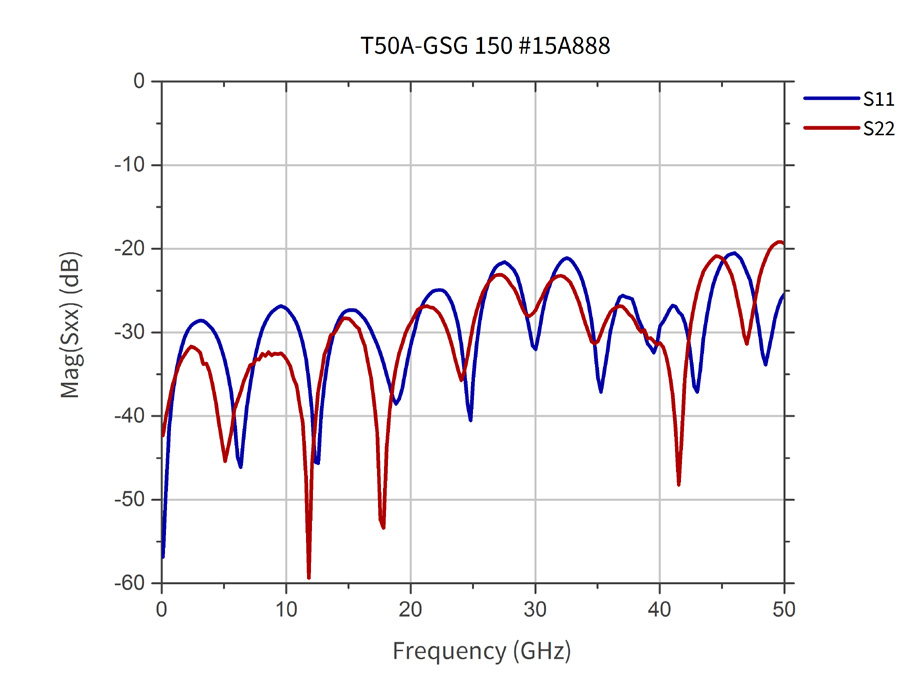
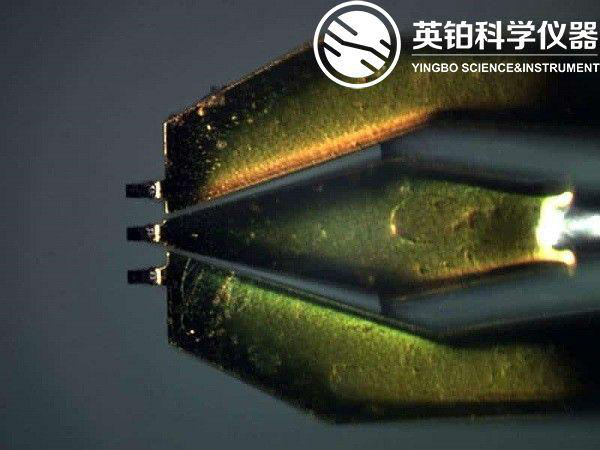
TITAN™ RF Probes are designed for advanced RF applications, offering unmatched calibration results and superior contact repeatability. They are optimized for on-wafer S-parameter measurements and RF power device characterization.
 Save to Favorites
Overview
Specifications
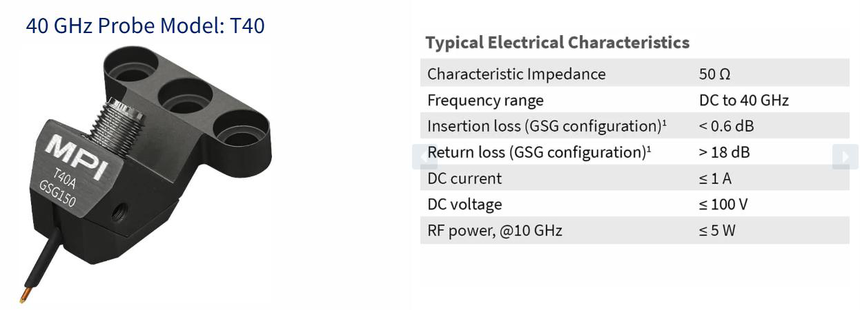
| Parameter | Value |
|---|---|
| Characteristic Impedance | 50Ω |
| Frequency Range | DC to 110GHz |
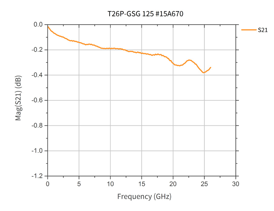
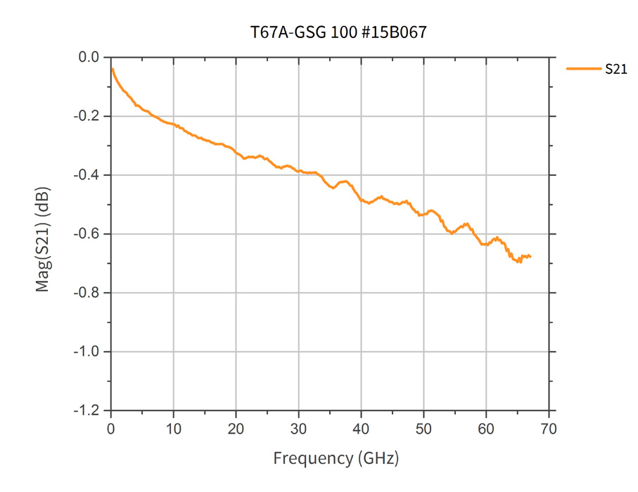
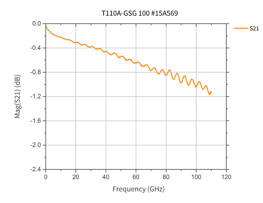
| Insertion Loss | <1.2dB |
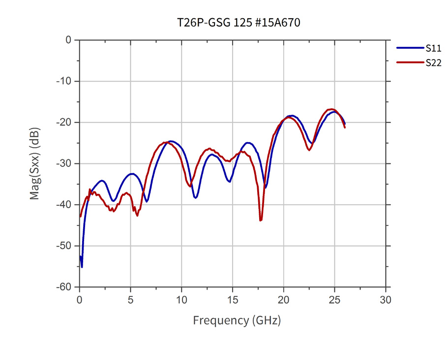
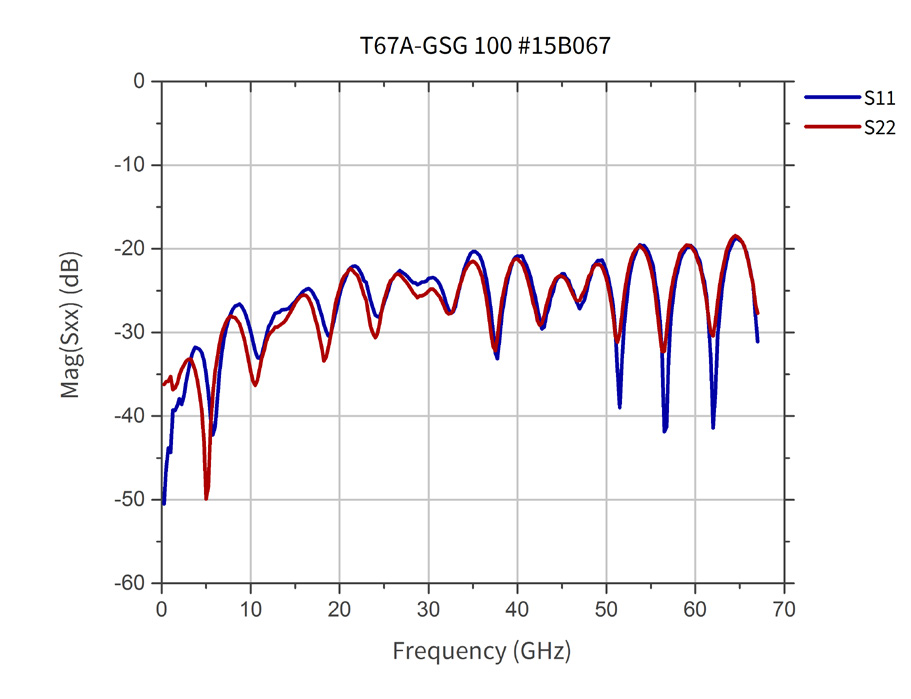
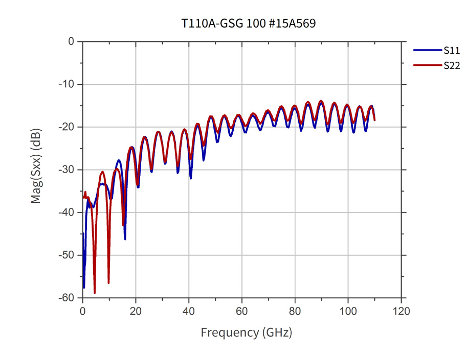
| Return Loss | >14dB |
| DC Current | ≤1A |
| DC Voltage | ≤100V |
| RF Power @10GHz | ≤5W |
| Thermal Range | -60 to 200°C |
| Connector | A (1mm) |
| Pitch Range | 50μm to 250μm |
| Standard Pitch Step | 25μm |
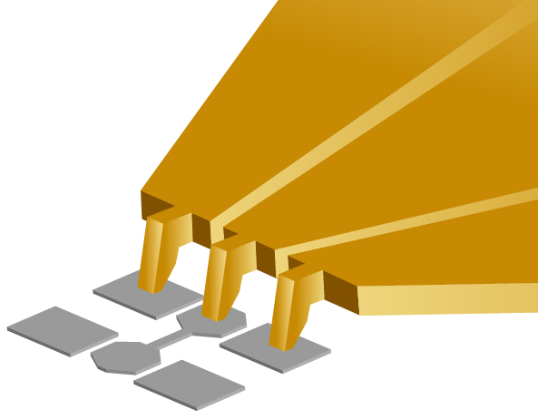
| Tip Configurations | GSG |
| Connector Angle | A-Style: 45-degree |
Applications
Key Features
Datasheet
Supplier Information
Related Products
-
 Unknown
Probe Station Accessories
Yokogawa
Unknown
Probe Station Accessories
Yokogawa
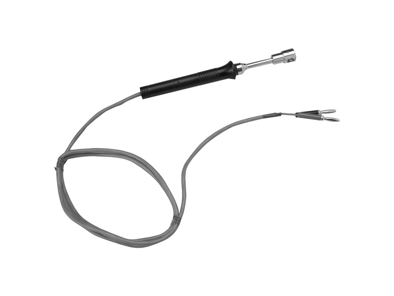
Cable Length: Unknown Connector Type: Unknown Material: Unknown
This product appears to be a specialized optical device, likely used for precision applications in the photonics industry.
-
 Type 8203 pH and ORP Probes
Probe Station Accessories
Burkert
Type 8203 pH and ORP Probes
Probe Station Accessories
Burkert
Measuring Range (mV): -2000...+2000 Fluid Temperature (°C): -10...+140
Type 8203 probes are designed for measuring pH or ORP in clean or contaminated liquids, including those with sulfides, proteins, or low conductivity.
-
 Unknown
Probe Station Accessories
Ybsemi-Solution
Unknown
Probe Station Accessories
Ybsemi-Solution
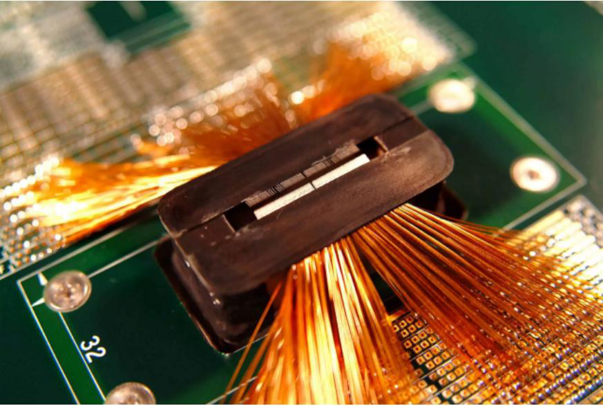
Number of Wires: Multiple Connection Type: High-density Operating Temperature: -40°C to +85°C
This product is a high-performance optical component designed for advanced electronic and photonic applications.
-
 TITAN™ Probe Family DC to 145 GHz
Probe Station Accessories
Ybsemi-Solution
TITAN™ Probe Family DC to 145 GHz
Probe Station Accessories
Ybsemi-Solution
Characteristic Impedance: 50Ω Connector Type: 0.8mm, female Tip Material: Ni alloy
The TITAN™ Probe Family offers unparalleled accuracy for single-ended and differential calibration, device, and circuit characterization across a wide frequency range up to 145 GHz.
-
 TITAN™ Probe Series
Probe Station Accessories
Ybsemi-Solution
TITAN™ Probe Series
Probe Station Accessories
Ybsemi-Solution
Characteristic Impedance: 50Ω Frequency Range: DC to 220GHz Insertion Loss (dB): <5
The TITAN™ Probe Series offers advanced RF probes designed for high-frequency and high-power applications. These probes are equipped with MEMS contact tips, ensuring unmatched calibration accuracy and reliability across a wide frequency range. They are ideal for RF testing, mmWave devices, and S-parameter measurements.
Related Articles
Founded in 2004, Wuhan Union Optic Inc. is a National Specialized, Refined, Unique & Innovative "Little Giant" high-tech enterprise located in Wuhan East Lake High-Tech Development Zone.
A solid-state laser is one of the most common and reliable laser types used in modern industry, medical equipment, and scientific research. Unlike gas or fiber lasers, it uses solid materials as its gain medium to generate stable, high-brightness laser beams. Thanks to its high precision, long lifespan, and compact structure, solid-state lasers have become a mainstream solution for high-precision laser processing and optical systems.
Electro-optic deflectors (EODs) are optical devices used to steer or deflect light beams by applying an electric field to a specialized optical crystal. Unlike mechanical beam steering systems that rely on moving mirrors, electro-optic deflectors enable high-speed, non-mechanical beam control with exceptional precision and responsiveness. They are widely used in laser scanning, optical communications, microscopy, laser printing, spectroscopy, and scientific research, where rapid and accurate laser beam positioning is essential.
In photonics and laser technology, devices that manipulate optical signals via the electro-optic effect form the backbone of precision optical systems. Electro-optic phase modulators and electro-optic deflectors are two prominent examples of this device category. As a critical hardware solution for high-speed, high-accuracy laser beam direction control, electro-optic deflectors are widely deployed across industrial and research settings. Below is a detailed overview of their core structure, key performance drivers, and primary use cases.
Loading...
Name
Phone
Organization
Use Case

Database Platform