
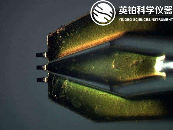
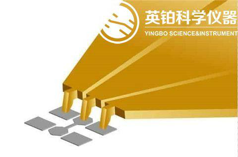
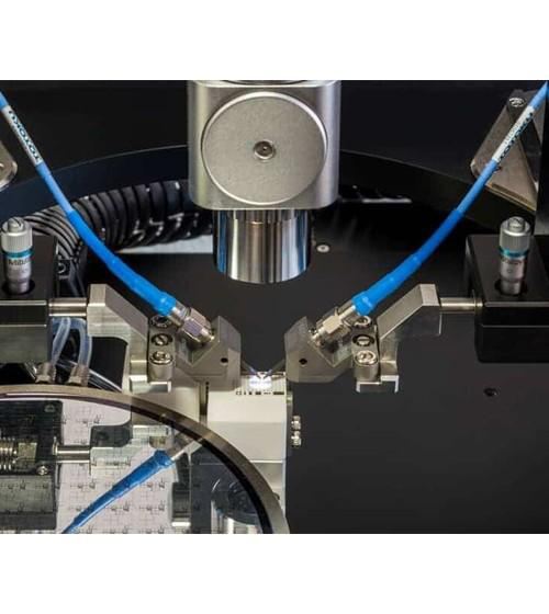
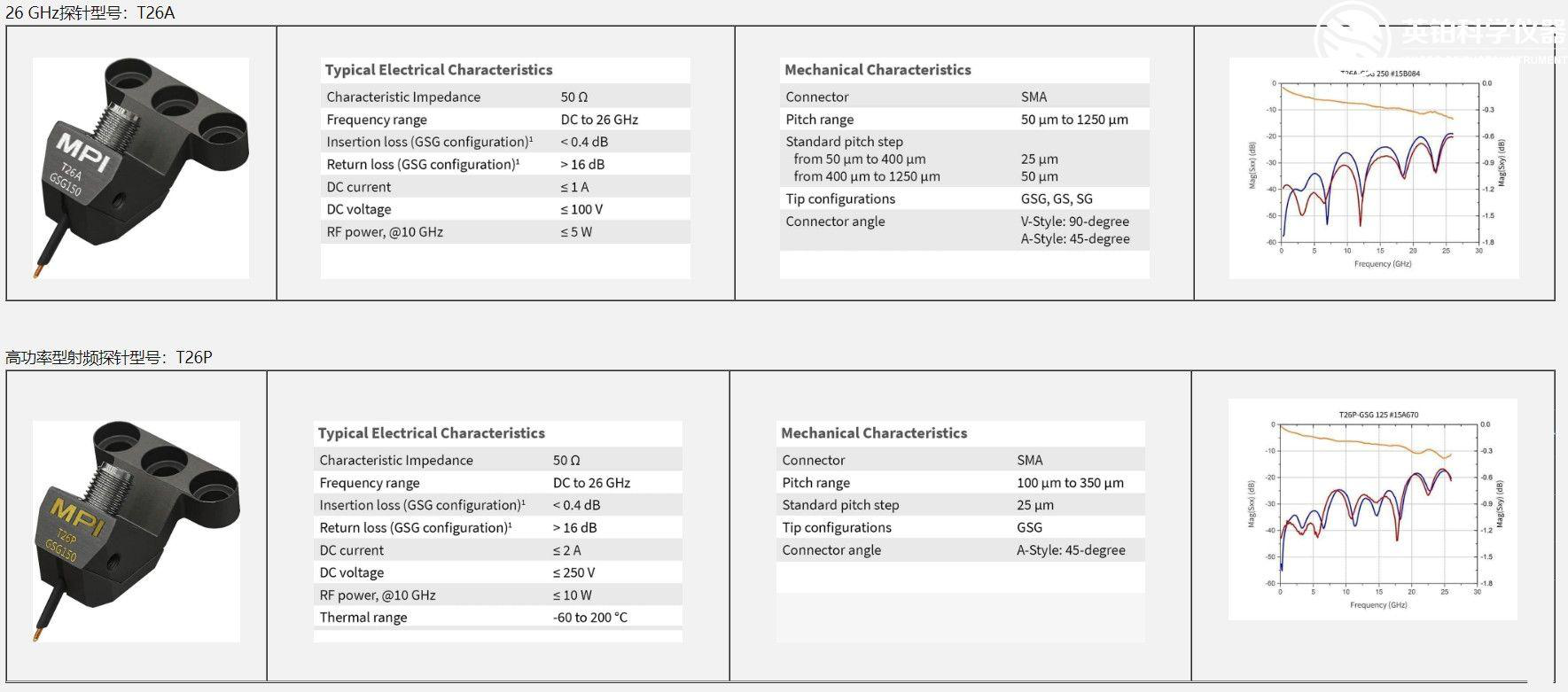
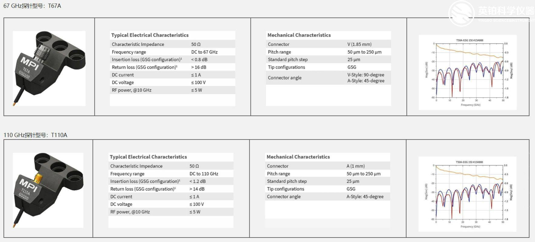
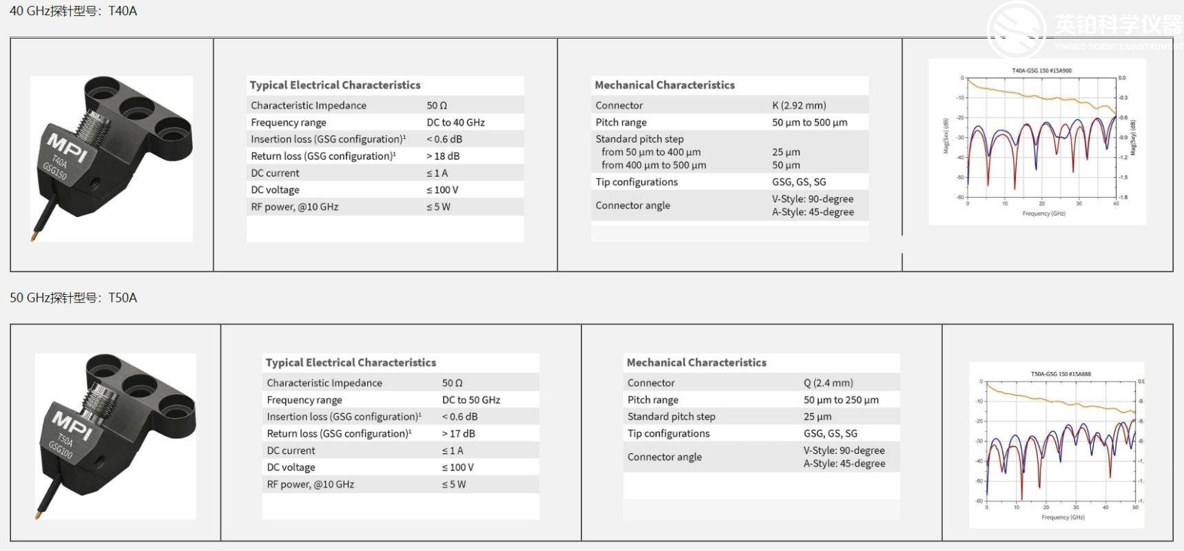
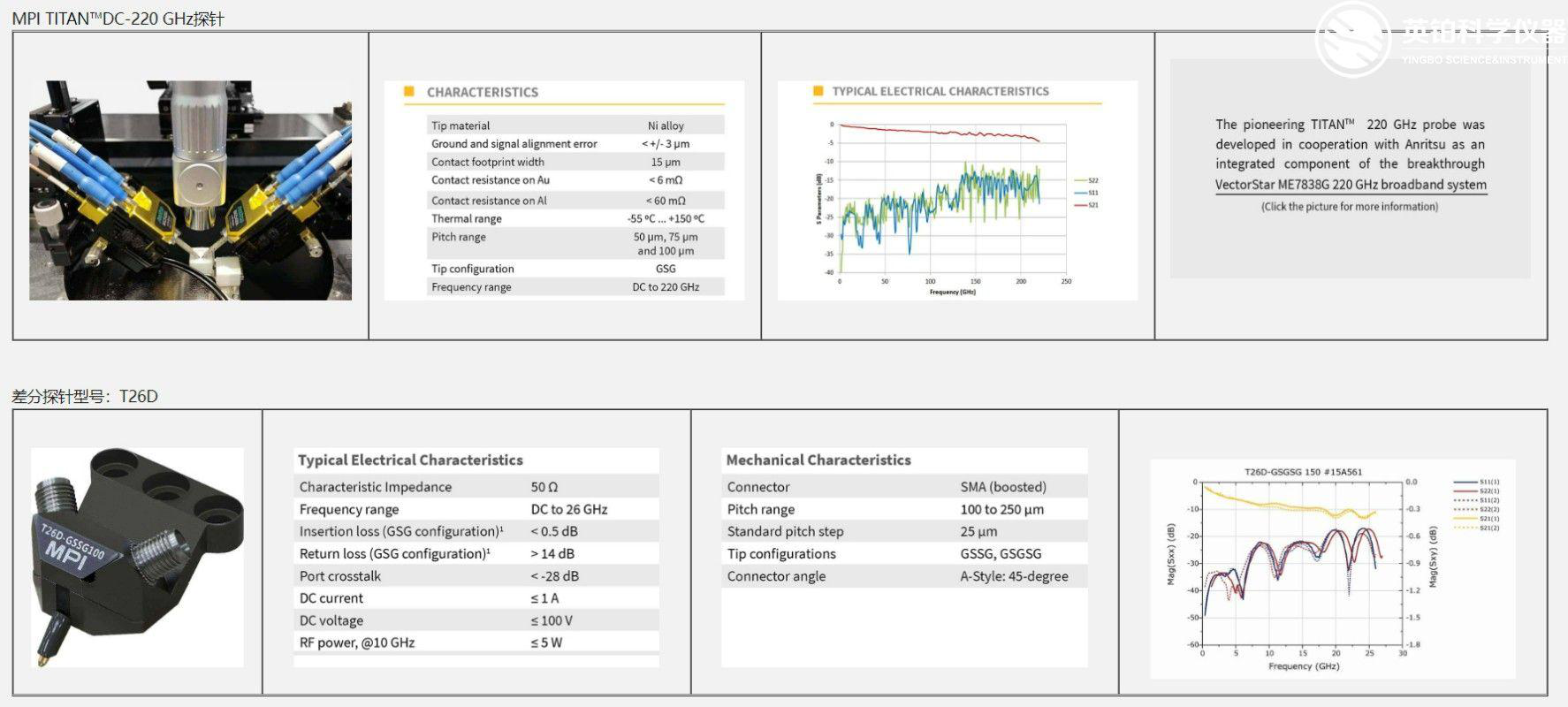
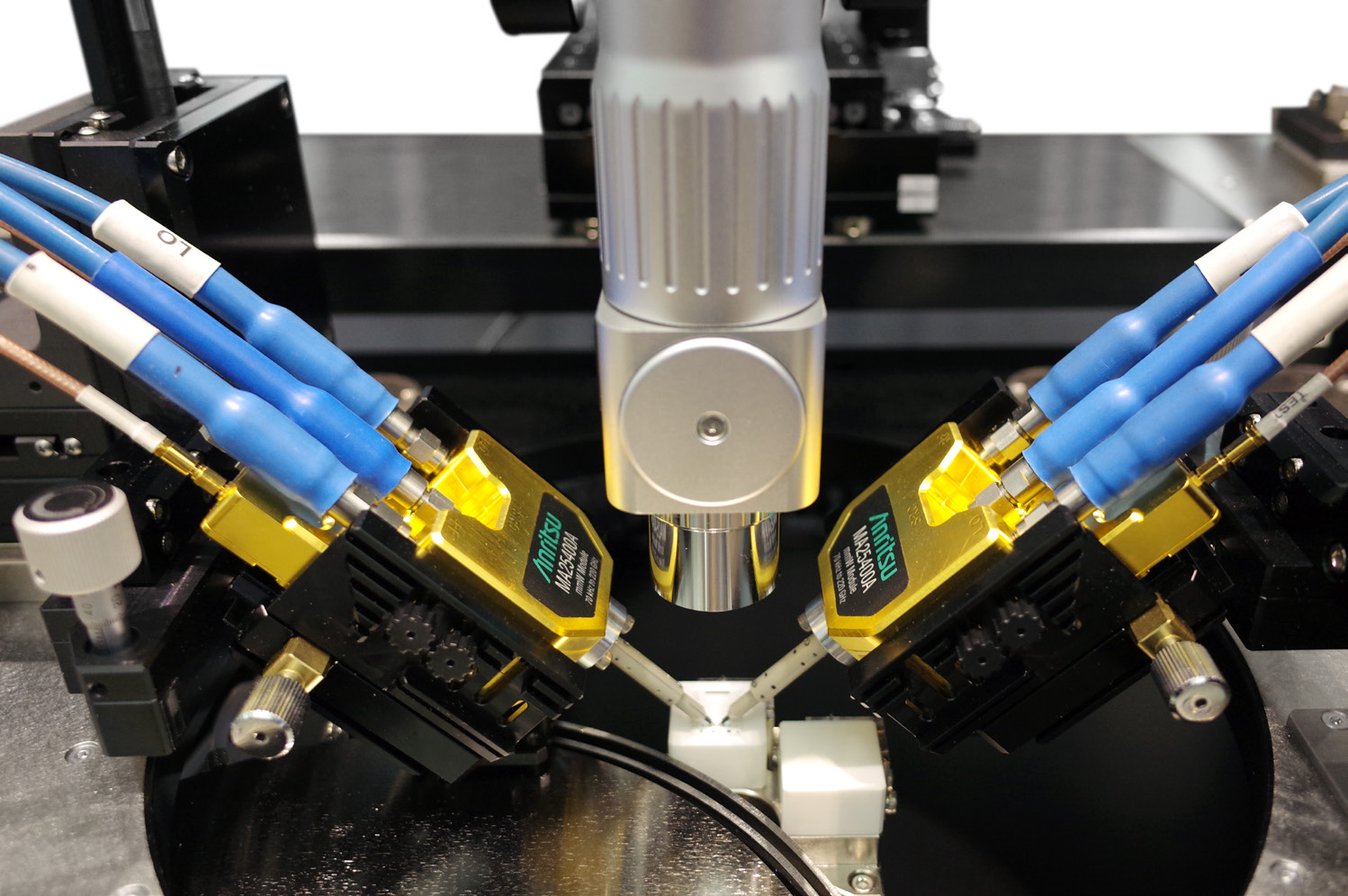

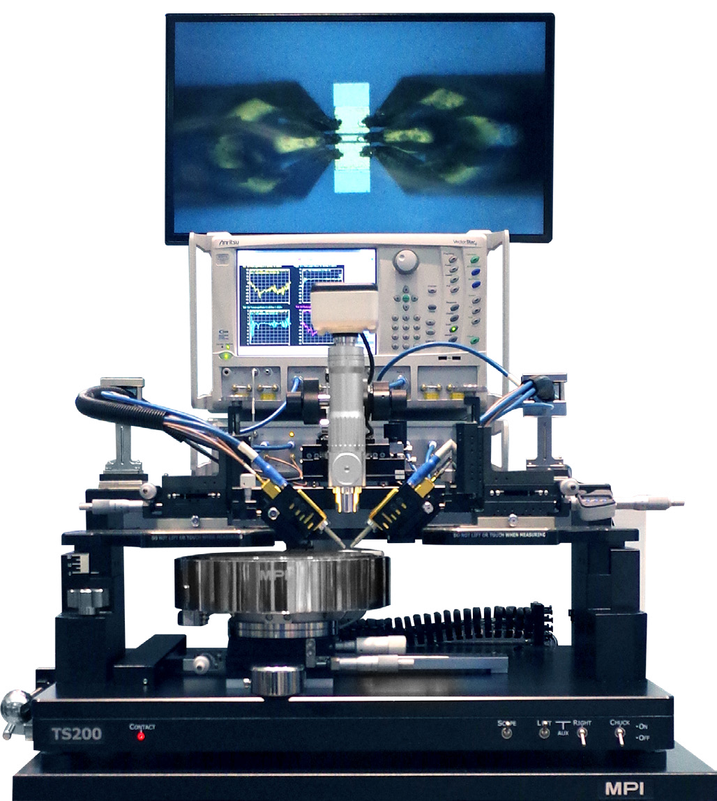
TITAN™ Probe Family DC to 145 GHz
The TITAN™ Probe Family offers unparalleled accuracy for single-ended and differential calibration, device, and circuit characterization across a wide frequency range up to 145 GHz.
 Save to Favorites
Overview
Specifications
| Parameter | Value |
|---|---|
| Characteristic Impedance | 50Ω |
| Connector Type | 0.8mm, female |
| Tip Material | Ni alloy |
| Contact Footprint Width | 15μm |
| Maximal Voltage | ≤50V |
| Maximal Current | ≤1.5A |
| Contact Resistance on Au | <6mΩ |
| Contact Resistance on Al | <45mΩ |
| Thermal Range | -40°C…+150°C |
| Frequency Range | DC to 145GHz |
| Pitch Range | 50, 75, 100, 125, and 150μm |
| Tip Configuration | GSG |
Applications
Key Features
Datasheet
Supplier Information
Related Products
-
 Unknown
Probe Station Accessories
Yokogawa
Unknown
Probe Station Accessories
Yokogawa
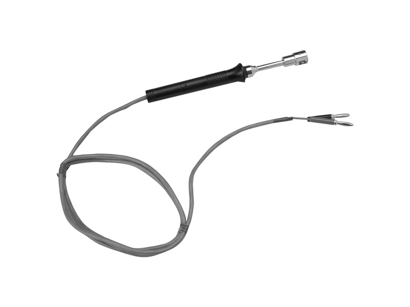
Cable Length: Unknown Connector Type: Unknown Material: Unknown
This product appears to be a specialized optical device, likely used for precision applications in the photonics industry.
-
 Type 8203 pH and ORP Probes
Probe Station Accessories
Burkert
Type 8203 pH and ORP Probes
Probe Station Accessories
Burkert
Measuring Range (mV): -2000...+2000 Fluid Temperature (°C): -10...+140
Type 8203 probes are designed for measuring pH or ORP in clean or contaminated liquids, including those with sulfides, proteins, or low conductivity.
-
 Unknown
Probe Station Accessories
Ybsemi-Solution
Unknown
Probe Station Accessories
Ybsemi-Solution
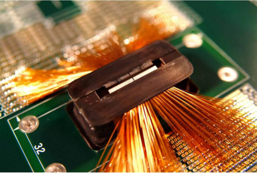
Number of Wires: Multiple Connection Type: High-density Operating Temperature: -40°C to +85°C
This product is a high-performance optical component designed for advanced electronic and photonic applications.
-
 TITAN™ Probe Series
Probe Station Accessories
Ybsemi-Solution
TITAN™ Probe Series
Probe Station Accessories
Ybsemi-Solution
Characteristic Impedance: 50Ω Frequency Range: DC to 220GHz Insertion Loss (dB): <5
The TITAN™ Probe Series offers advanced RF probes designed for high-frequency and high-power applications. These probes are equipped with MEMS contact tips, ensuring unmatched calibration accuracy and reliability across a wide frequency range. They are ideal for RF testing, mmWave devices, and S-parameter measurements.
Related Articles
Electro-optic deflectors (EODs) are optical devices used to steer or deflect light beams by applying an electric field to a specialized optical crystal. Unlike mechanical beam steering systems that rely on moving mirrors, electro-optic deflectors enable high-speed, non-mechanical beam control with exceptional precision and responsiveness. They are widely used in laser scanning, optical communications, microscopy, laser printing, spectroscopy, and scientific research, where rapid and accurate laser beam positioning is essential.
An infrared transmitter (IR transmitter) is a basic electronic component that sends invisible infrared light signals for short-range wireless control. It is widely used in daily electronics, smart home devices, and industrial equipment due to its low cost, low power consumption, and stable performance.
Shanghai Connet Laser Technology Co., Ltd. focuses on technological innovation, delivering cutting-edge photonic products & solutions for industrial lasers, LiDAR, fiber optic sensing, coherent telecom, cold atom physics and precision spectroscopy research & mass manufacturing.
Wuhan Optical Valley Interlink Technology Co., Ltd. was founded in 2013 by a technical team from Huazhong University of Science and Technology.
Loading...
Name
Phone
Organization
Use Case

Database Platform