
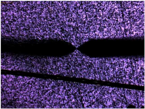
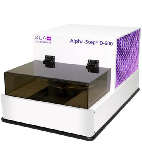
Alpha-Step D-600
The Alpha-Step D-600 is a high-performance surface profiler designed for precise measurement of step heights, roughness, and thin film thickness. It is widely used in research and industrial applications for material characterization.
 Save to Favorites
Overview
Specifications
| Parameter | Value |
|---|---|
| Measurement Range | 0.1nm to 1200μm |
| Resolution | 0.01nm |
| Scan Speed | up to 200μm/s |
| Sample Size | up to 200mm diameter |
| Repeatability | ±0.5% |
| Data Acquisition Rate | up to 50kHz |
| Optical System | High-resolution camera with advanced optics |
| Software Features | Automated analysis and reporting |
Applications
Key Features
Datasheet
Supplier Information
Related Products
-
 OPS-1000 3D Optical Profiler
Optical Surface Profiler
Santec
OPS-1000 3D Optical Profiler
Optical Surface Profiler
Santec
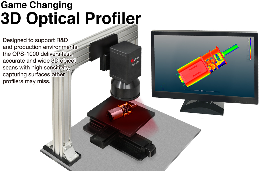
Scanning Range: Wide Sensitivity: High Scanning Speed: Fast
The OPS-1000 is designed to support R&D and production environments, delivering fast, accurate, and wide 3D object scans with high sensitivity, capturing surfaces other profilers may miss.
-
 Keyence Laser Displacement Sensor
Optical Surface Profiler
Keyence
Keyence Laser Displacement Sensor
Optical Surface Profiler
Keyence
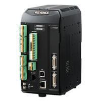
Measuring Range: 20mm-200mm Resolution: 0.01mm Sampling Speed: 80kHz
The Keyence Laser Displacement Sensor is a high-precision measurement device designed for accurate distance and position detection in various industrial applications.
-
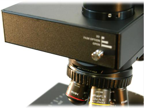 Zeta-300
Optical Surface Profiler
Ybsemi-Solution
Zeta-300
Optical Surface Profiler
Ybsemi-Solution
Scanning Range: 280μm Sample Stage Size: 150×150mm, 200×200mm, 300×300mm Imaging Resolution: 5MP
Zeta-300 is a fast, non-contact 3D optical profiler designed for precise surface measurement and analysis.
-
 Tencor P-170 Stylus Profiler
Optical Surface Profiler
Ybsemi-Solution
Tencor P-170 Stylus Profiler
Optical Surface Profiler
Ybsemi-Solution
Scan Length: ≤200mm Vertical Range: ≤1mm Force Control Range: 0.03g-50g
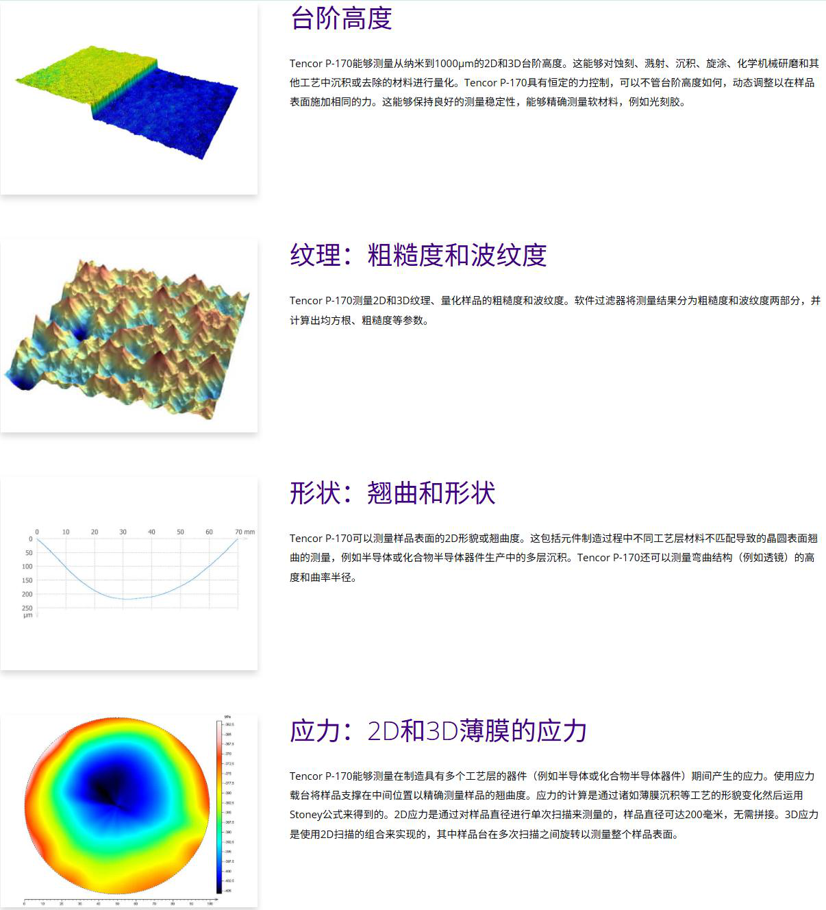
The Tencor P-170 Stylus Profiler is a cassette-to-cassette system designed for high-precision surface measurement. It offers advanced capabilities for 2D and 3D scanning, step height measurement, roughness analysis, and thin film stress evaluation, making it ideal for semiconductor, LED, MEMS, and data storage applications.
-
 Zeta-388 Optical Profiler
Optical Surface Profiler
Ybsemi-Solution
Zeta-388 Optical Profiler
Optical Surface Profiler
Ybsemi-Solution
Optical Resolution: 5MP Sample Size Range: 45×35μm to 9.5×7.5mm Film Thickness Range: 30nm to 100μm
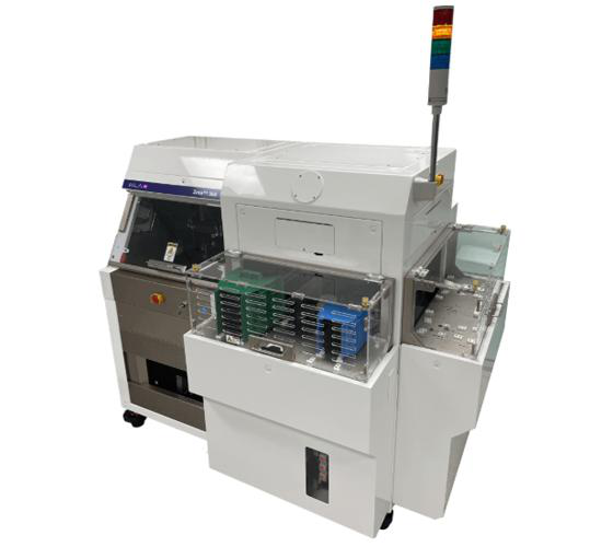
The Zeta-388 optical profiler is a non-contact, 3D surface topography measurement system designed for automated defect inspection and precise measurements of step heights, roughness, and film thickness. It features ZDot™ technology and multi-mode optics for high-resolution imaging.
Related Articles
VCSEL, short for Vertical Cavity Surface Emitting Laser, is a widely used semiconductor laser component in modern optoelectronics. Unlike traditional edge-emitting lasers, VCSEL emits laser light vertically from its chip surface. Thanks to its low power consumption, stable beam quality, low cost, and easy integration, it has become the core light source for 3D sensing, wearable devices, and high-speed optical communication.
Founded in Beijing in 2011, Beijing FJR Opto-electronic Technology Co., Ltd. specializes in R&D, manufacturing and sales of infrared thermal imaging equipment and complete optoelectronic systems.
In photonics and laser technology, devices that manipulate optical signals via the electro-optic effect form the backbone of precision optical systems. Electro-optic phase modulators and electro-optic deflectors are two prominent examples of this device category. As a critical hardware solution for high-speed, high-accuracy laser beam direction control, electro-optic deflectors are widely deployed across industrial and research settings. Below is a detailed overview of their core structure, key performance drivers, and primary use cases.
Founded in 2019, Jilin JC Ultrafast Equipment Co., Ltd. is a high-tech enterprise incubated by the Ultrafast Optoelectronics Center of Jilin University. Our R&D team owns 15 years of profound experience in femtosecond laser micro-nano fabrication.
Loading...
Name
Phone
Organization
Use Case

Database Platform