
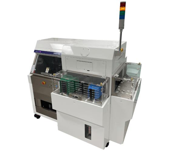
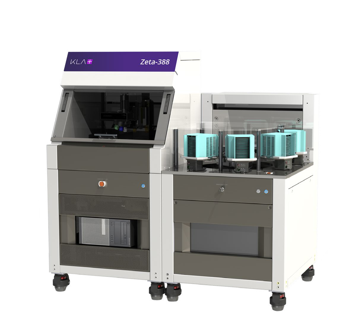
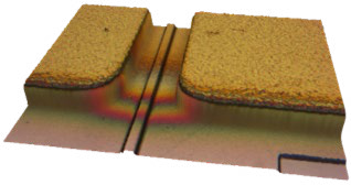

Zeta-388 Optical Profiler
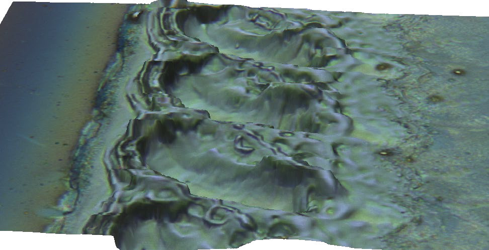
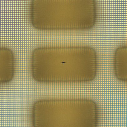
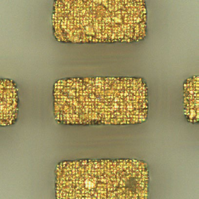
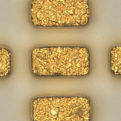
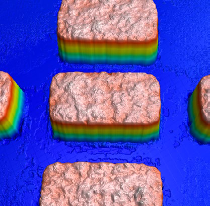
The Zeta-388 optical profiler is a non-contact, 3D surface topography measurement system designed for automated defect inspection and precise measurements of step heights, roughness, and film thickness. It features ZDot™ technology and multi-mode optics for high-resolution imaging.
 Save to Favorites
Overview
Specifications
| Parameter | Value |
|---|---|
| Optical Resolution | 5MP |
| Sample Size Range | 45×35μm to 9.5×7.5mm |
| Film Thickness Range | 30nm to 100μm |
| Step Height Measurement Range | up to 250nm |
| Stage Size | 200mm motorized XY stage |
| Scanning Modes | Brightfield, darkfield, differential image contrast (DIC) |
| Autofocus | Enabled |
| Light Source Type | Broadband white light or 405nm monochromatic LED |
| Sample Loading | 100, 150, and 200mm wafers |
| Vibration Isolation | Built-in vibration isolation and acoustic enclosure |
Applications
Key Features
Datasheet
Supplier Information
Related Products
-
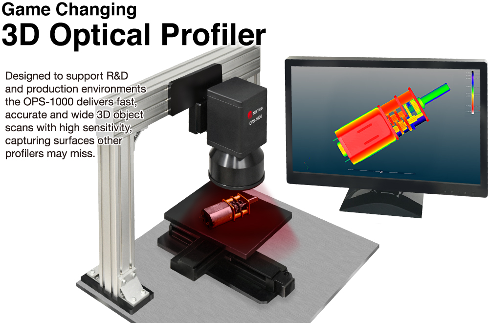 OPS-1000 3D Optical Profiler
Optical Surface Profiler
Santec
OPS-1000 3D Optical Profiler
Optical Surface Profiler
Santec
Scanning Range: Wide Sensitivity: High Scanning Speed: Fast
The OPS-1000 is designed to support R&D and production environments, delivering fast, accurate, and wide 3D object scans with high sensitivity, capturing surfaces other profilers may miss.
-
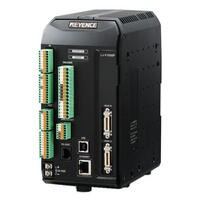 Keyence Laser Displacement Sensor
Optical Surface Profiler
Keyence
Keyence Laser Displacement Sensor
Optical Surface Profiler
Keyence
Measuring Range: 20mm-200mm Resolution: 0.01mm Sampling Speed: 80kHz
The Keyence Laser Displacement Sensor is a high-precision measurement device designed for accurate distance and position detection in various industrial applications.
-
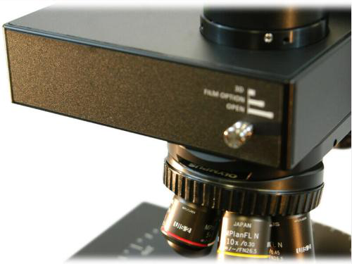 Zeta-300
Optical Surface Profiler
Ybsemi-Solution
Zeta-300
Optical Surface Profiler
Ybsemi-Solution
Scanning Range: 280μm Sample Stage Size: 150×150mm, 200×200mm, 300×300mm Imaging Resolution: 5MP
Zeta-300 is a fast, non-contact 3D optical profiler designed for precise surface measurement and analysis.
-
 Tencor P-170 Stylus Profiler
Optical Surface Profiler
Ybsemi-Solution
Tencor P-170 Stylus Profiler
Optical Surface Profiler
Ybsemi-Solution
Scan Length: ≤200mm Vertical Range: ≤1mm Force Control Range: 0.03g-50g
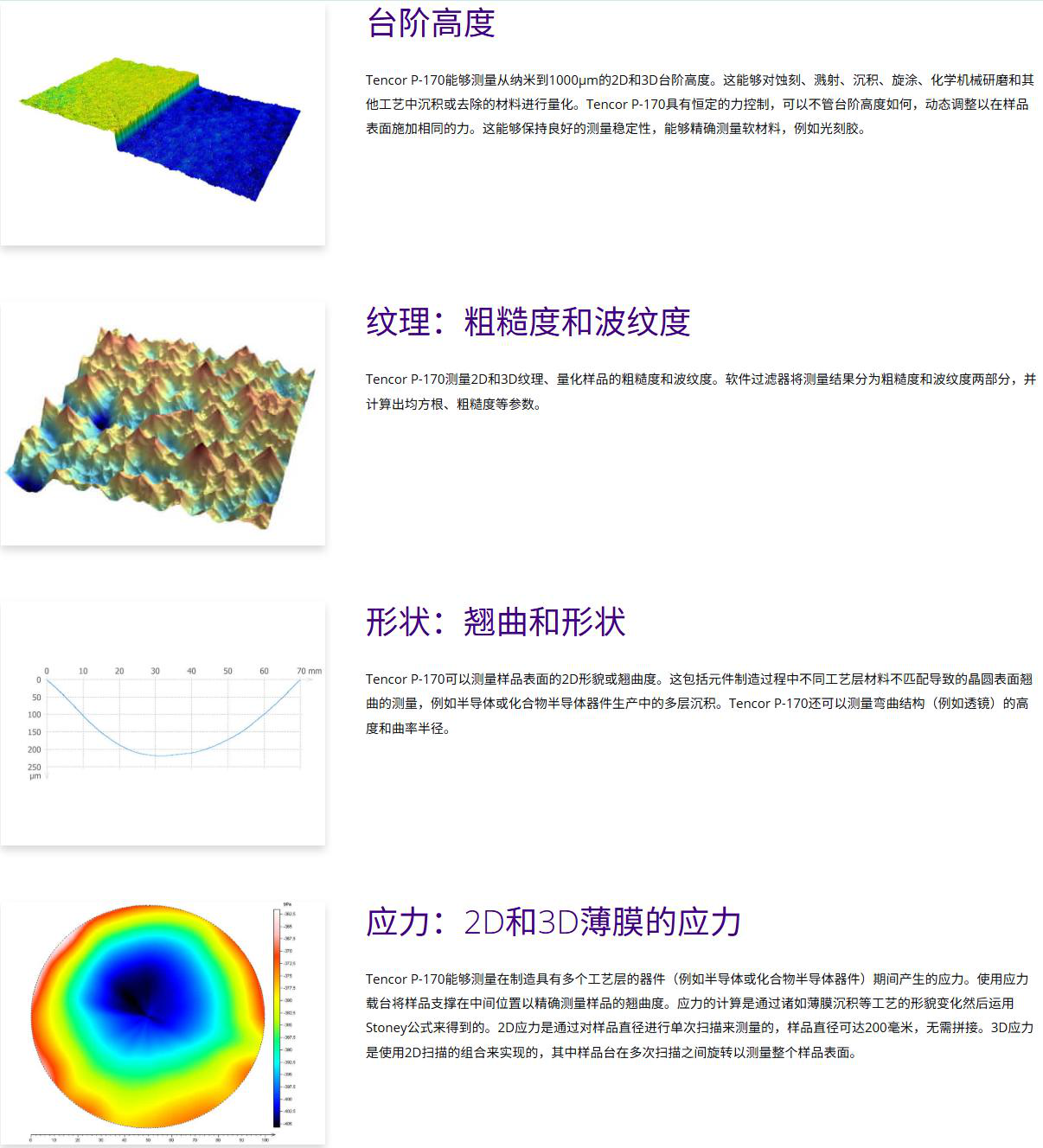
The Tencor P-170 Stylus Profiler is a cassette-to-cassette system designed for high-precision surface measurement. It offers advanced capabilities for 2D and 3D scanning, step height measurement, roughness analysis, and thin film stress evaluation, making it ideal for semiconductor, LED, MEMS, and data storage applications.
Related Articles
Electro-optic deflectors (EODs) are optical devices used to steer or deflect light beams by applying an electric field to a specialized optical crystal. Unlike mechanical beam steering systems that rely on moving mirrors, electro-optic deflectors enable high-speed, non-mechanical beam control with exceptional precision and responsiveness. They are widely used in laser scanning, optical communications, microscopy, laser printing, spectroscopy, and scientific research, where rapid and accurate laser beam positioning is essential.
An infrared transmitter (IR transmitter) is a basic electronic component that sends invisible infrared light signals for short-range wireless control. It is widely used in daily electronics, smart home devices, and industrial equipment due to its low cost, low power consumption, and stable performance.
Shanghai Connet Laser Technology Co., Ltd. focuses on technological innovation, delivering cutting-edge photonic products & solutions for industrial lasers, LiDAR, fiber optic sensing, coherent telecom, cold atom physics and precision spectroscopy research & mass manufacturing.
Wuhan Optical Valley Interlink Technology Co., Ltd. was founded in 2013 by a technical team from Huazhong University of Science and Technology.
Loading...
Name
Phone
Organization
Use Case

Database Platform