

ETHOS NX5000
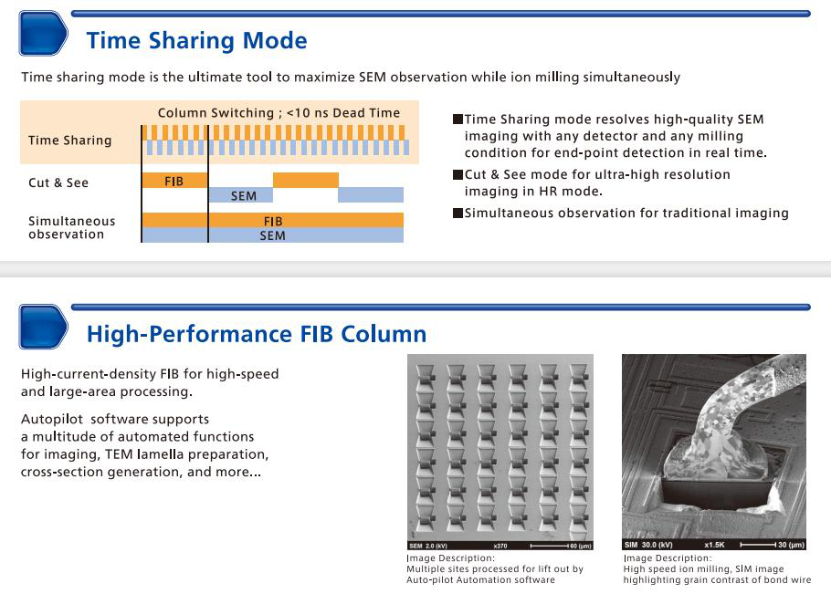
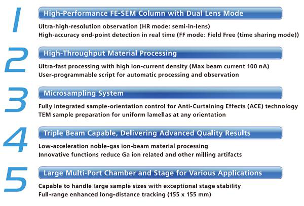
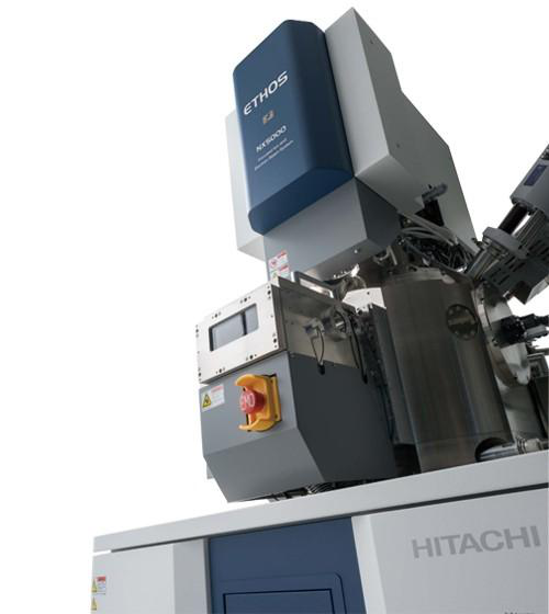
ETHOS NX5000 is a high-performance focused ion beam scanning electron microscope (FE-SEM) designed for advanced material processing and imaging applications.
 Save to Favorites
Overview
Specifications
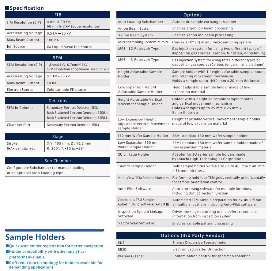
| Parameter | Value |
|---|---|
| SIM Resolution (C,P) | 4nm@30kV, 60nm@2kV (Edge resolution) |
| Accelerating Voltage | 0.1kV–30kV |
| Max Beam Current | 10nA |
| Ion Source | Ga Liquid Metal Ion Source |
| SEM Resolution (C,P) | 1.5nm@1kV, 0.7nm@15kV SEM resolution at optimum Imaging WD |
| Electron Source | Cold cathode FE source |
| Stroke | X,Y: 155mm, Z: 16.5mm, R: 360°, T: -10° to +59° |
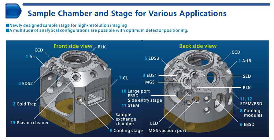
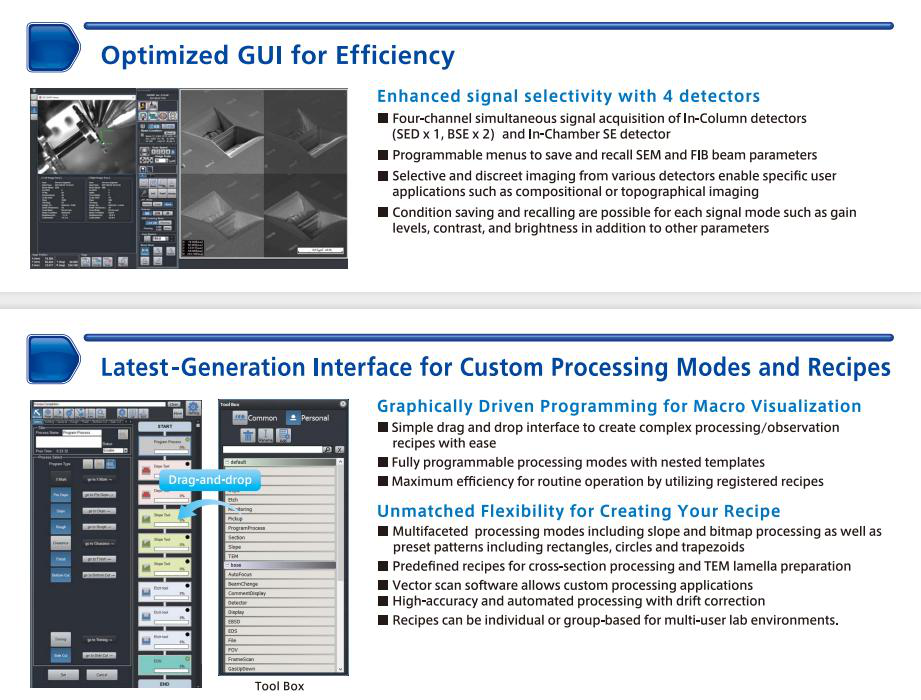
| Detectors | SEM In-Column: Secondary Electron Detector (SE(U)), Back Scattered Electron Detector (BSE(U)), Back Scattered Electron Detector (BSE(L)) |
| Chamber Port | Secondary Electron Detector (SE(L)) |
| Sub-Chamber | Configurable Subchamber for manual loading or an optional Auto-Loading type |
Applications
Key Features
Datasheet
Supplier Information
Related Products
-
 SU8600 Series Scanning Electron Microscope
Material Analysis and Forensics
Ybsemi-Solution
SU8600 Series Scanning Electron Microscope
Material Analysis and Forensics
Ybsemi-Solution
Secondary Electron Resolution: 0.6nm@15kV, 0.7nm@1kV Magnification: 20-2,000,000× Electron Gun: 冷阴极场发射枪, 支持技术间活动Function, Includes 低噪声模块系统
The SU8600 series scanning electron microscope offers high-resolution imaging and advanced analytical capabilities, suitable for various applications in materials science, semiconductor inspection, and biological research.
-
 PHEMOS-X
Material Analysis and Forensics
Ybsemi-Solution
PHEMOS-X
Material Analysis and Forensics
Ybsemi-Solution
Main Unit Dimensions: 1656mm(W)×2000mm(H)×1247mm(D) Main Unit Weight: Approx.1640kg Operation Desk Dimensions 1: 1000mm(W)×700mm(H)×800mm(D)
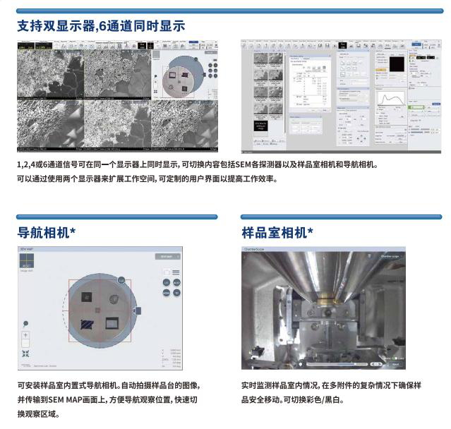
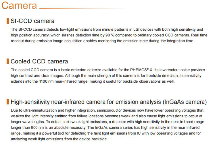
PHEMOS-X is a high-performance emission analysis system designed for detecting low-light emissions from semiconductor devices with high sensitivity and precision. It features advanced cameras, display functions, and optical stage capabilities.
-
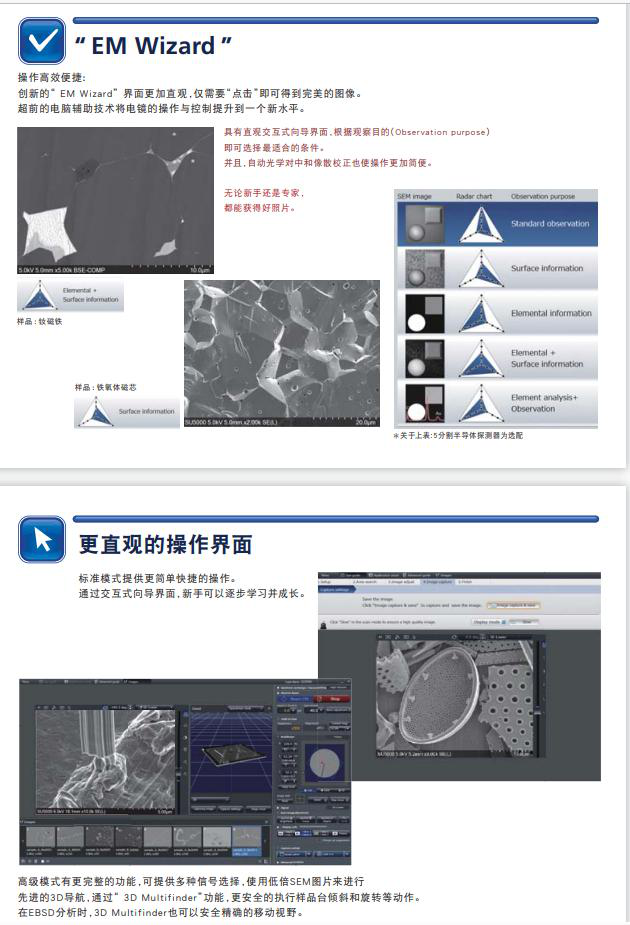 SU5000 Scanning Electron Microscope
Material Analysis and Forensics
Ybsemi-Solution
SU5000 Scanning Electron Microscope
Material Analysis and Forensics
Ybsemi-Solution
Resolution 1.2nm@30kV(SE): 1.2nm Resolution 3.0nm@1kV(SE): 3.0nm Resolution 2.0nm@1kV(SE): 2.0nm
The SU5000 Scanning Electron Microscope (SEM) offers advanced imaging capabilities with intuitive operation, enabling users to achieve high-quality images efficiently.
-
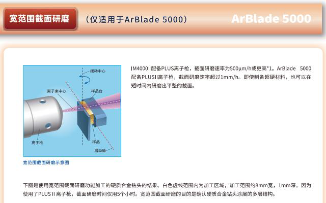 IM4000 II & ArBlade 5000
Material Analysis and Forensics
Ybsemi-Solution
IM4000 II & ArBlade 5000
Material Analysis and Forensics
Ybsemi-Solution
Gas Source: 氩气 Gas Flow Control Method: 质量流量控制 Acceleration Voltage: IM4000 II: 0.0~6.0kV, ArBlade 5000: 0.0~8.0kV
IM4000 II and ArBlade 5000 are advanced ion milling systems designed for precise surface preparation and analysis. They offer high-speed milling capabilities and versatile applications for various materials.
-
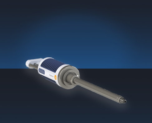 Unknown
Material Analysis and Forensics
Kyky
Unknown
Material Analysis and Forensics
Kyky
Unknown Parameter: Unknown
This is a high-precision optical device designed for specialized applications, offering advanced performance and reliability.
Related Articles
Shanghai Connet Laser Technology Co., Ltd. focuses on technological innovation, delivering cutting-edge photonic products & solutions for industrial lasers, LiDAR, fiber optic sensing, coherent telecom, cold atom physics and precision spectroscopy research & mass manufacturing.
A solid-state laser is one of the most common and reliable laser types used in modern industry, medical equipment, and scientific research. Unlike gas or fiber lasers, it uses solid materials as its gain medium to generate stable, high-brightness laser beams. Thanks to its high precision, long lifespan, and compact structure, solid-state lasers have become a mainstream solution for high-precision laser processing and optical systems.
Looking for a market-verified 808nm pump laser diode? This guide introduces HAUCORE DM-8E5A-8OD (HGLD-808-COS-D-5W), its core advantages, key specs and mainstream industrial, medical & research applications.
Founded in 2003, BWT Beijing Optoelectronics adheres to the mission "Let Dreams Fly With Light" and vision of becoming a Global Leader in Laser Solutions, guided by the core value "Innovate to Achieve Extraordinary".
Loading...
Name
Phone
Organization
Use Case

Database Platform