

Apex XCT
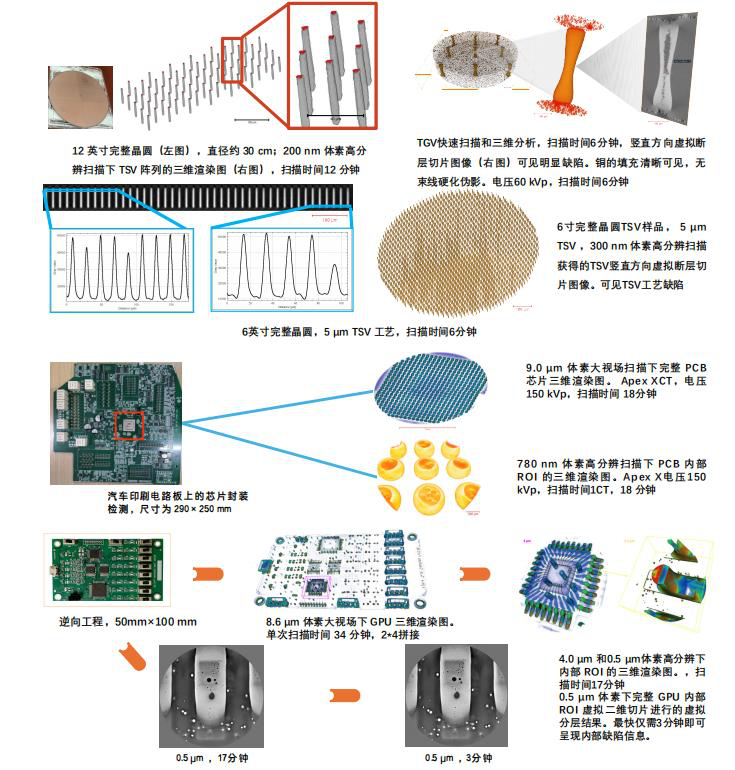
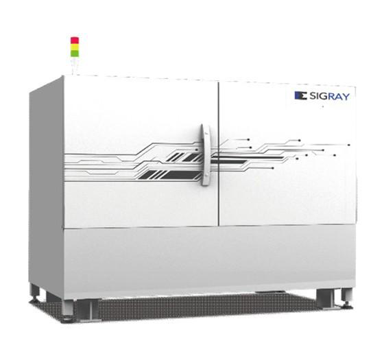
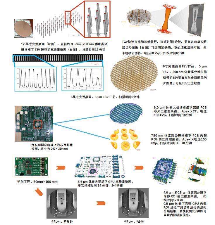
Apex XCT is a high-throughput, sub-micron resolution 3D X-ray CT system designed for precise imaging and analysis of various samples, including PCBs, soft batteries, and crystalline samples.
 Save to Favorites
Overview
Specifications
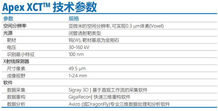
| Parameter | Value |
|---|---|
| Spatial Resolution | Sub-micron spatial resolution, achieving 0.3μm voxel |
| X-ray Source | Rotating anode transmission type |
| Target Material | Tungsten (W), diamond substrate |
| Voltage | 30-160kV |
| Minimum Feature Recognition | 100nm |
| X-ray Detector Pixel Size | 49.5μm |
| Imaging Field of View | 1-24mm |
| Data Acquisition | Sigray 3D software based on workflow |
| Data Reconstruction | GigaRecon high-speed 3D reconstruction software |
| Data Analysis | Avizo (or DragonFly) professional 3D data processing and analysis software |
Applications
Key Features
Datasheet
Supplier Information
Related Products
-
 Apex XCT
3D Scanner
Ybsemi-Solution
Apex XCT
3D Scanner
Ybsemi-Solution
Spatial Resolution: Sub-micron resolution, 0.3μm voxel X-ray Source: Transmission type Target Material: Tungsten (W), diamond substrate
Apex XCT is a high-throughput, sub-micron resolution 3D X-ray CT system designed for rapid and precise imaging of various samples, including PCBs, soft-pack batteries, and crystalline samples.
-
 surfaceCONTROL 3D 3500
3D Scanner
Micro-Epsilon
surfaceCONTROL 3D 3500
3D Scanner
Micro-Epsilon
Maximum Repeatability: 0.25μm Best Z-Axis Resolution: 0.7μm Up to 2.2 million 3D data points per second: 220万点
The surfaceCONTROL 3D 3500 is a high-precision 3D sensor designed for inline shape and surface inspection. It offers exceptional measurement accuracy and resolution, making it ideal for automated quality control in industrial applications.
-
 surfaceCONTROL 3D 3500
3D Scanner
Micro-Epsilon
surfaceCONTROL 3D 3500
3D Scanner
Micro-Epsilon
Maximum Repeatability: 0.25μm Best Z-Axis Resolution: 0.7μm 3D Data Points per Second: 2200000
High-precision inline 3D measurement sensor designed for surface inspection and shape analysis.
Related Articles
Electro-optic deflectors (EODs) are optical devices used to steer or deflect light beams by applying an electric field to a specialized optical crystal. Unlike mechanical beam steering systems that rely on moving mirrors, electro-optic deflectors enable high-speed, non-mechanical beam control with exceptional precision and responsiveness. They are widely used in laser scanning, optical communications, microscopy, laser printing, spectroscopy, and scientific research, where rapid and accurate laser beam positioning is essential.
An infrared transmitter (IR transmitter) is a basic electronic component that sends invisible infrared light signals for short-range wireless control. It is widely used in daily electronics, smart home devices, and industrial equipment due to its low cost, low power consumption, and stable performance.
Shanghai Connet Laser Technology Co., Ltd. focuses on technological innovation, delivering cutting-edge photonic products & solutions for industrial lasers, LiDAR, fiber optic sensing, coherent telecom, cold atom physics and precision spectroscopy research & mass manufacturing.
Wuhan Optical Valley Interlink Technology Co., Ltd. was founded in 2013 by a technical team from Huazhong University of Science and Technology.
Loading...
Name
Phone
Organization
Use Case

Database Platform