What Is a Linear CCD Image Sensor? Working Principle & Key Applications of Toshiba TCD1304DG
Published: 2026-08-05 15:30:40 Views: 93
1. Why Choose Linear CCD Image Sensors
For 1D optical detection scenarios such as spectrum acquisition, dimensional measurement and optical scanning, area array CMOS/CCD suffer redundant pixels, high cost and slow row readout speed. Low-pixel linear sensors lack resolution, carry high dark current and easily saturate under strong light, failing high-precision, wide-dynamic continuous sampling requirements.
A linear CCD image sensor is a single-column 1D photoelectric chip. It converts light into electric charge via photodiodes and outputs serial analog signals through CCD analog shift registers. Featuring high resolution, superior sensitivity and adjustable integration exposure, it is specially designed for one-dimensional optical paths and continuous scanning equipment.
Toshiba TCD1304DG is a mainstream commercial 3648-pixel high-performance linear CCD with built-in electronic shutter and sample & hold circuit. It delivers ultra-low dark current and wide dynamic range with 3.0V low-voltage operation and 22-pin hermetic CERDIP package, acting as the core light sensing component for spectrometers, industrial dimensional inspection and optical metrology instruments.
2. Working Principle of Linear CCD Image Sensors
Taking Toshiba TCD1304DG dual-channel shift register linear CCD as an example, the full signal acquisition workflow includes four stages: photoelectric conversion, charge accumulation, electronic shutter reset and serial charge readout.
- Photoelectric Conversion: The chip integrates 3648 PN photodiodes. Incident light generates photocharge proportional to light intensity and integration time. Each pixel measures 8 μm × 200 μm with 8 μm center-to-center pitch for high-density sampling.
- Integration & Electronic Shutter (ICG): The ICG integration clear gate serves as electronic shutter to rapidly discharge residual charge on photodiodes. Minimum integration time reaches 10 μs, eliminating saturation distortion under high illumination without mechanical moving parts.
- Charge Transfer & Storage: Generated photocharge is shifted into two parallel CCD analog shift registers via SH shift gate for temporary storage, minimizing signal crosstalk with maximum register imbalance of only 3%.
- Sample & Hold Signal Output: On-chip sample & hold circuit buffers charge, which is amplified and output as analog voltage from the OS pin. The master clock φM controls readout speed up to 1 MHz to complete full readout of all 3648 effective pixels.
Separate digital (VDD) and analog (VAD) power supplies isolate digital noise to protect weak optical signals.
3. Core Product Highlights of Toshiba TCD1304DG
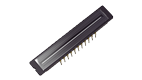
- High 3648 effective pixels: Single-column dense sensing array with 8 μm pixel pitch, greatly improving resolution for high-precision spectroscopy and dimensional measurement;
- High sensitivity & ultra-low dark current: Typical sensitivity of 160 V/lx·s, maximum dark signal voltage limited to 5 mV for excellent SNR under weak light; typical dynamic range of 300 supports both dim and bright light acquisition;
- Built-in ICG electronic shutter: No extra mechanical shutter required, minimum integration time 10 μs to suppress saturation and image lag for pulsed and high-brightness light sources;
- Low-voltage dual power supply: Minimum 3.0V for digital & analog power rails, standard operating voltage 4V with typical power consumption of 25 mW, simplifying low-power equipment design;
- Fully integrated on-chip circuits: Embedded CCD drive logic, sample & hold circuit and output buffer reduce external peripheral hardware complexity;
- Consistent optical response: Photo response non-uniformity (PRNU) ≤10%, register imbalance (RI) ≤3% for stable, repeatable measurement data;
- Wide operating temperature range: Operating temperature -25 ℃ ~ +60 ℃, storage temperature -40 ℃ ~ +100 ℃, stable performance in industrial workshops and laboratory environments;
- Hermetic 22-pin CERDIP ceramic package: Resists moisture and mechanical deformation with stable window transmittance; standard through-hole layout for easy PCB soldering and integration.
4. Key Product Applications
- Spectroscopy Instruments: UV-Vis spectrophotometers, Raman spectrometers, fiber spectrometers for 400–1100 nm spectral curve capture;
- Industrial 1D Dimensional Inspection: Real-time scanning measurement of sheet width, wire diameter, film thickness and web edge position;
- Optical Metrology & Calibration: Beam profile analyzers, radiant luminance calibration equipment, light power distribution testing;
- Printing & Packaging Inspection: High-speed barcode scanning, printing color difference detection, paper defect screening via 1D scanning;
- Academic Laboratory Optical Platforms: Interference & diffraction experiments, monochromator supporting optical sensing modules;
- Material Sorting Equipment: Continuous on-line detection of material color difference and transmittance of transparent substrates.