
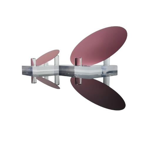
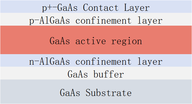
Gallium Arsenide Epitaxial LED
Epitaxial P/N/MQW Layers on GaAs,Primarily IR/NIR Emission700–1100nm.
 Save to Favorites
Overview
Specifications
| Parameter | Value |
|---|---|
| GaAs Red LED Epitaxy (2~6 Inches) - Substrate Diameter | 2 inch - 50.8mm |
| GaAs Red LED Epitaxy (2~6 Inches) - Substrate Diameter | 4 inch - 100mm |
| GaAs Red LED Epitaxy (2~6 Inches) - Substrate Diameter | 6 inch - 150mm |
| GaAs Red LED Epitaxy (2~6 Inches) - GaAs Substrate Thickness [Substrate diameter: 2 inch - 50.8mm] | 350μm |
| GaAs Red LED Epitaxy (2~6 Inches) - GaAs Substrate Thickness [Substrate diameter: 4 inch - 100mm] | 1000μm |
| GaAs Red LED Epitaxy (2~6 Inches) - GaAs Substrate Thickness [Substrate diameter: 6 inch - 150mm] | 1000μm |
| Gallium Arsenide Red LED Epitaxy (2~6 Inches) - Gallium Arsenide Substrate Surface | Polished/Etched |
| Gallium Arsenide Red LED Epitaxy (2~6 Inches) - Gallium Arsenide Substrate Crystal Orientation | (100) 15°Off Toward <111> ±0.5° |
| Gallium Arsenide Red LED Epitaxy (2~6 Inches) - Gallium Arsenide Substrate Model | N-Si |
| Gallium Arsenide Red LED Epitaxy (2~6 Inches) - Epitaxial Emission Type | Red LED Light |
| Gallium Arsenide Red LED Epitaxy (2~6 Inches) - Emission Wavelength | 570-655nm |
Applications
Datasheet
Please provide your email to download the datasheet.
Invalid email format. Please try again.
Supplier Information
Related Products
-
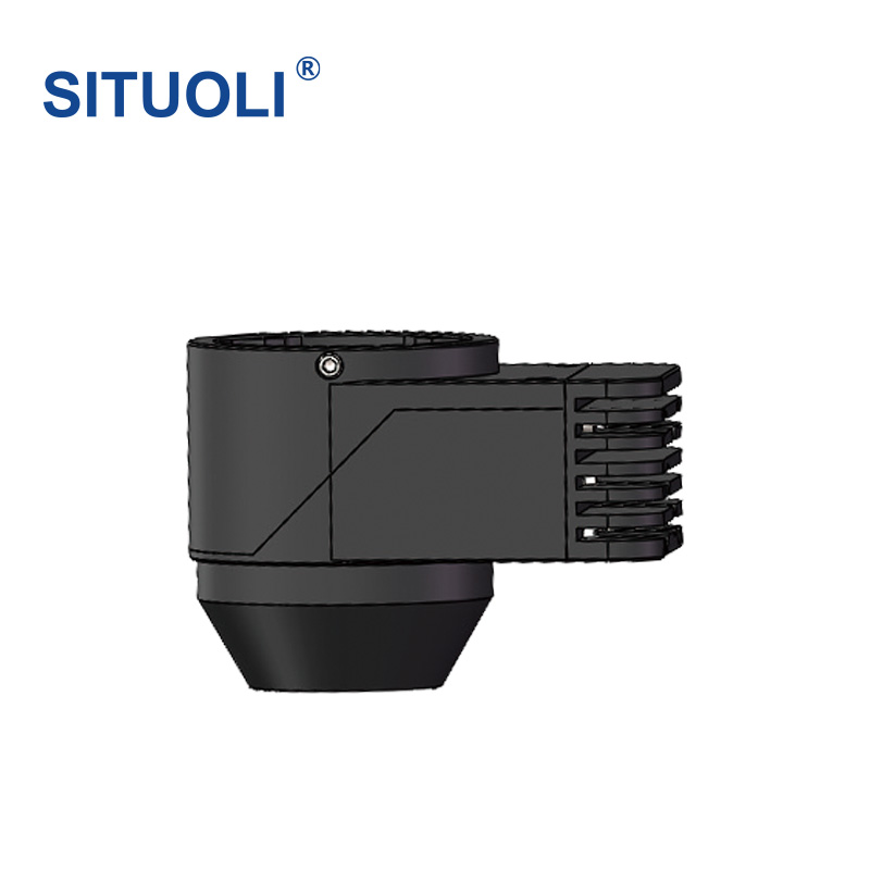 Monochromatic LED Fluorescence Module STL-MOFL-U
Light-Emitting Diodes (LEDs)
Situoli
Light Source: 10W Adjustable LED Service Life: >60000 小时 Light-Intensity Control Range: 0%~100% Linear Adjustment
SITUOLI's monochromatic LED illumination unit provides brightfield or fluorescence illumination for upright microscopes. Stable performance and efficient fluorescence illumination serve varied applications. A short optical path increases brightness and fluorescence excitation efficiency for better signal detection; adjustable intensity reduces photobleaching. The specially designed LED source lasts 60,000 hours. Combined with objectives, tube lenses, camera interfaces and cameras, it forms a direct microscopy imaging system. Advanced STL-IMCS video/image-processing software supplied with the camera supports life-science and other research. It integrates into automation such as automatic slide readers and pathology slide scanners, primarily for fungal, microbial and gynecological testing.
-
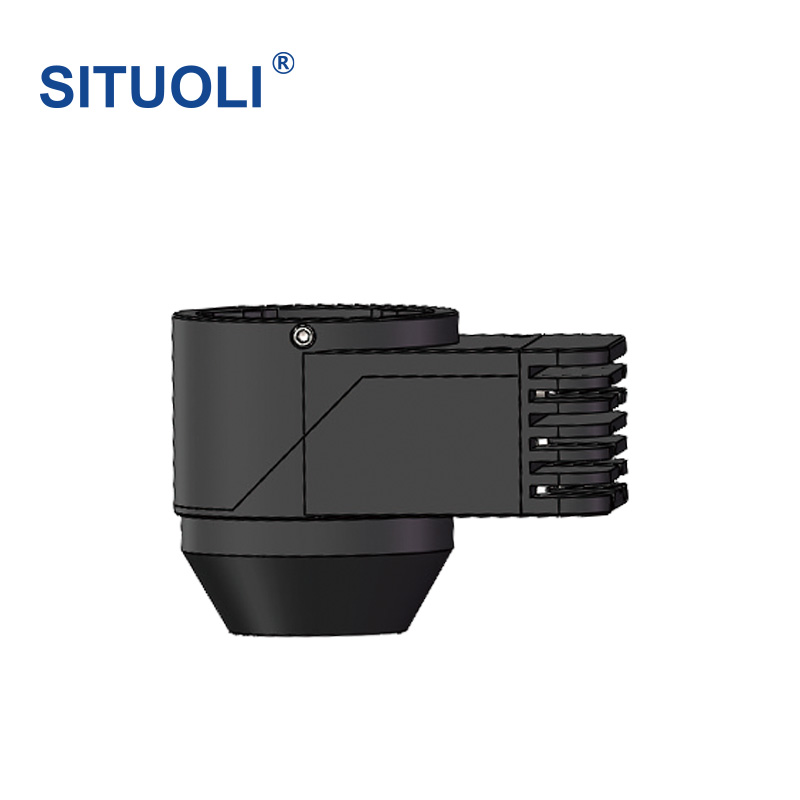 Monochromatic LED Fluorescence Module STL-MOFL-B
Light-Emitting Diodes (LEDs)
Situoli
Light Source: 10W Adjustable LED Service Life: >60000 小时 Light-Intensity Control Range: 0%~100% Linear Adjustment
SITUOLI's monochromatic LED illumination unit provides brightfield or fluorescence illumination for upright microscopes. Stable performance and efficient fluorescence illumination serve varied applications. A short optical path increases brightness and fluorescence excitation efficiency for better signal detection; adjustable intensity reduces photobleaching. The specially designed LED source lasts 60,000 hours. Combined with objectives, tube lenses, camera interfaces and cameras, it forms a direct microscopy imaging system. Advanced STL-IMCS video/image-processing software supplied with the camera supports life-science and other research. It integrates into automation such as automatic slide readers and pathology slide scanners, primarily for fungal, microbial and gynecological testing.
-
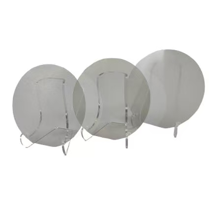 Sapphire-Based GaN Epitaxial LED
Light-Emitting Diodes (LEDs)
Jmwafer
Sapphire-Based GaN LED Epitaxy (2~8 Inches) - Substrate Diameter: 50.8 mm Sapphire-Based GaN LED Epitaxy (2~8 Inches) - Substrate Diameter: 100mm Sapphire-Based GaN LED Epitaxy (2~8 Inches) - Substrate Diameter: 150mm
Sapphire-Based Epitaxial GaN LED Is a Light-Emitting Diode with GaN Grown on Sapphire.
-
 Silicon-Based GaN Epitaxial LED
Light-Emitting Diodes (LEDs)
Jmwafer
Silicon-Based GaN LED Epitaxy (2~8 Inches) - Substrate Diameter: 50.8mm Silicon-Based GaN LED Epitaxy (2~8 Inches) - Substrate Diameter: 100mm Silicon-Based GaN LED Epitaxy (2~8 Inches) - Substrate Diameter: 150mm
GaN-on-Si LED Epitaxy Combines Efficient GaN Emission/Low-Cost Silicon for LED Chips,Important Research Direction.
Related Articles
The accelerated construction of new‑generation power systems has brought revolutionary upgrades to power‑equipment maintenance workflows.
Driven by fast‑growing demands of 3D perception, biometric authentication and machine‑vision industries, near‑infrared imaging optics have become a vital hardware component for intelligent sensing systems.
icrolight is a high-tech enterprise specializing in the R&D, manufacturing and sales of active and passive photonic devices for microwave photonics, LiDAR ranging, gas sensing, fiber optics and photomedicine.
Electro-optic deflectors (EODs) are optical devices used to steer or deflect light beams by applying an electric field to a specialized optical crystal. Unlike mechanical beam steering systems that rely on moving mirrors, electro-optic deflectors enable high-speed, non-mechanical beam control with exceptional precision and responsiveness. They are widely used in laser scanning, optical communications, microscopy, laser printing, spectroscopy, and scientific research, where rapid and accurate laser beam positioning is essential.
Loading...
Name
Phone
Organization
Use Case

Database Platform