
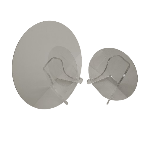
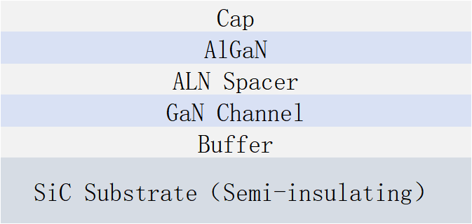
Silicon-Carbide-Based GaN Epitaxial HEMT
GaN-on-SiC HEMT Epitaxy Combines GaN High-Frequency/Power with SiC Thermal Conductivity by Growing GaN Films on SiC.
 Save to Favorites
Overview
Specifications
| Parameter | Value |
|---|---|
| Silicon-Carbide-Based GaN HEMT Epitaxial Substrate (2~6 Inches) - Substrate Diameter | 2 inch - 50.8mm |
| Silicon-Carbide-Based GaN HEMT Epitaxial Substrate (2~6 Inches) - Substrate Diameter | 4 inch - 100mm |
| Silicon-Carbide-Based GaN HEMT Epitaxial Substrate (2~6 Inches) - Substrate Diameter | 6 inch - 150mm |
| Silicon-Carbide-Based GaN HEMT Epitaxial Substrate (2~6 Inches) - Silicon Carbide Substrate Thickness [Substrate diameter: 2 inch - 50.8mm] | 500μm |
| Silicon-Carbide-Based GaN HEMT Epitaxial Substrate (2~6 Inches) - Silicon Carbide Substrate Thickness [Substrate diameter: 4 inch - 100mm] | 500μm |
| Silicon-Carbide-Based GaN HEMT Epitaxial Substrate (2~6 Inches) - Silicon Carbide Substrate Thickness [Substrate diameter: 6 inch - 150mm] | 500μm |
| Silicon-Carbide-Based GaN HEMT Epitaxial Substrate (2~6 Inches) - Silicon Carbide Substrate Crystal Orientation | {0001} |
| Silicon-Carbide-Based GaN HEMT Epitaxial Substrate (2~6 Inches) - Silicon Carbide Substrate Resistivity | ≥1E7 Ω·cm |
Applications
Datasheet
Please provide your email to download the datasheet.
Invalid email format. Please try again.
Supplier Information
Related Products
-
 Lithium Tantalate Wafer LT
Optical Crystals
Jmwafer
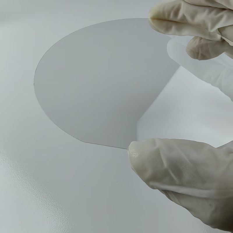
Diameter [Lithium Tantalate Single-Crystal Substrate LiTaO3/LT (2~6 Inches)]: 2 inch - 50.8mm Diameter [Lithium Tantalate Single-Crystal Substrate LiTaO3/LT (2~6 Inches)]: 3 inch - 76.2mm Diameter [Lithium Tantalate Single-Crystal Substrate LiTaO3/LT (2~6 Inches)]: 4 inch - 100mm
LiTaO₃ Usually Colorless/Pale Yellow,Trigonal Distorted-Perovskite Structure,Excellent Electro-Optic,Piezoelectric/Pyroelectric Properties.
-
 Lithium Niobate Wafer LN
Optical Crystals
Jmwafer
Diameter [Lithium Niobate Single-Crystal Substrate LiNbO3/LN (2~6 Inches)]: 2 inch - 50.8mm Diameter [Lithium Niobate Single-Crystal Substrate LiNbO3/LN (2~6 Inches)]: 3 inch - 76.2mm Diameter [Lithium Niobate Single-Crystal Substrate LiNbO3/LN (2~6 Inches)]: 4 inch - 100mm
LiNbO₃ Trigonal,Good Symmetry/Structural Stability,Piezoelectric,Ferroelectric,Photoelectric,Acousto-Optic/Nonlinear Properties,Curie up to1140℃,High Mechanical Quality/Chemical Stability.
-
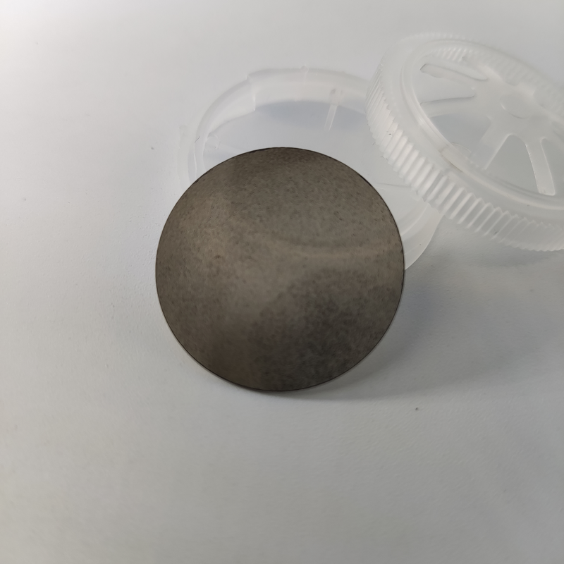 Polycrystalline Diamond
Optical Crystals
Jmwafer
Polycrystalline Diamond - Dimensions: 10 mm × 10 mm Polycrystalline Diamond - Dimensions: 1 inch - 25.4mm Polycrystalline Diamond - Dimensions: 2 inch - 50.8mm
Diamond:Tetrahedrally Packed Carbon,Extremely Hard,Excellent Thermal Conductivity/Broad Optical Transparency,Hardest Known Natural Material,Also Synthesized at High Pressure/Temperature.
-
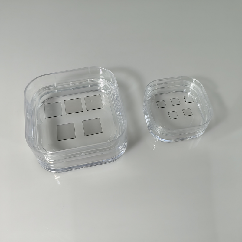 Single-Crystal Diamond
Optical Crystals
Jmwafer
Single-Crystal Diamond - Diameter: 5 mm × 5 mm Single-Crystal Diamond - Diameter: 10 mm × 10 mm Single-Crystal Diamond - Diameter: 20 mm × 20 mm
Diamond:Tetrahedrally Packed Carbon,Extremely Hard,Excellent Thermal Conductivity/Broad Optical Transparency,Hardest Known Natural Material,Also Synthesized at High Pressure/Temperature.
-
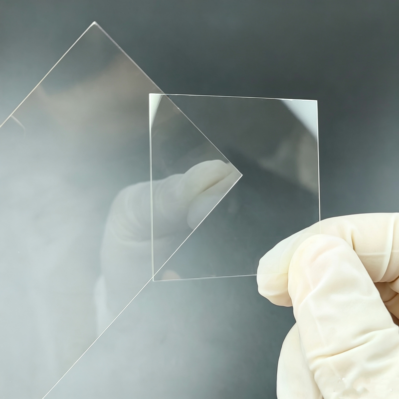 Fluorophlogopite
Optical Crystals
Jmwafer
Fluoromica Substrate - Dimensions: 5 mm × 5 mm Fluoromica Substrate - Dimensions: 10 mm × 10 mm Fluoromica Substrate - Dimensions: 20 mm × 20 mm
Synthetic Fluorophlogopite Mica KMg3(AlSi3O10)F2,Melts1375℃/Long-Term up to1100℃,Colorless Transparent,Strong Acid-Alkali Inert,Stable/Pure/Complete Structure/Flat Cleavage,Easily Split Thin.
Related Articles
Raybowlaser, a professional manufacturer of high-power laser chips, has officially launched its upgraded new-generation 1470nm high-performance laser chip. Achieving groundbreaking progress in rated output power and wall-plug efficiency (WPE), this innovative laser chip delivers superior and reliable core light source solutions for medical cosmetology, industrial processing, agricultural applications and scientific research equipment.
Electro-optic deflectors (EODs) are optical devices used to steer or deflect light beams by applying an electric field to a specialized optical crystal. Unlike mechanical beam steering systems that rely on moving mirrors, electro-optic deflectors enable high-speed, non-mechanical beam control with exceptional precision and responsiveness. They are widely used in laser scanning, optical communications, microscopy, laser printing, spectroscopy, and scientific research, where rapid and accurate laser beam positioning is essential.
Founded in 2004, Wuhan Union Optic Inc. is a National Specialized, Refined, Unique & Innovative "Little Giant" high-tech enterprise located in Wuhan East Lake High-Tech Development Zone.
Precise spectral screening is essential for high-precision medical detection, spectroscopic analysis and intelligent imaging systems. Tailored for visible and near-infrared spectral separation, the SP900 shortpass optical filter delivers high-efficiency light transmission and deep infrared blocking performance. It effectively eliminates stray light interference, improves signal-to-noise ratio (SNR), and serves as a core optical component for biomedical instruments, scientific analysis equipment and machine vision systems.
Loading...
Name
Phone
Organization
Use Case

Database Platform