
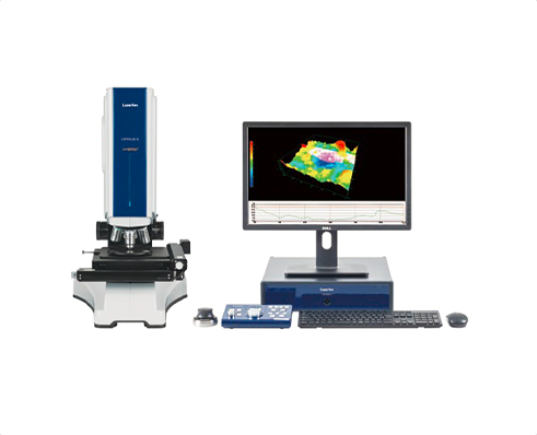
Laser and White Light Confocal Microscope C3
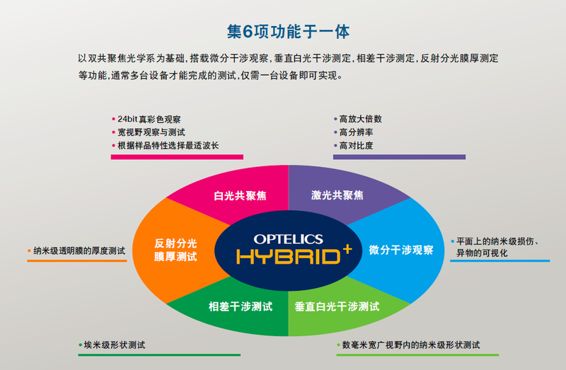
Lasertec, Japan, introduced the OPTELICS Hybrid confocal microscope, combining laser and white light sources for versatile, high performance confocal microscopy. Two sets of confocal optics work with accessories including an interferometer, differential interference contrast observation and spectral reflectance film thickness measurement. Lasertec is a Japanese semiconductor inspection equipment company founded in 1960, primarily supplying semiconductor wafer and photomask…
 Save to Favorites
Overview
Specifications
| Parameter | Value |
|---|---|
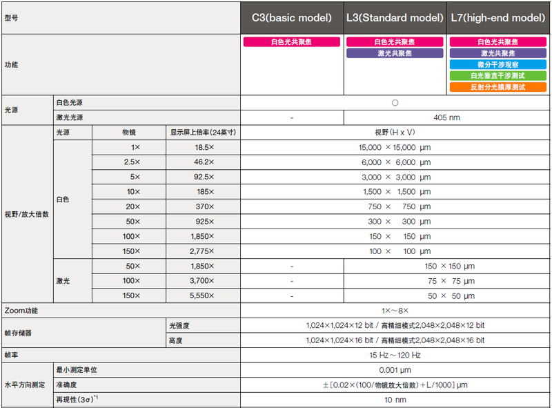
| Zoom Magnification | 1×–8× |
| Light Intensity Frame Storage | 1024×1024×12bit; High Definition mode 2048×2048×12bit |
| Height Frame Storage | 1024×1024×16bit; High Definition mode 2048×2048×16bit |
| Frame Rate | 15–120 Hz |
| Minimum Horizontal Measurement Increment | 0.001 μm |
| Horizontal Accuracy | ±[0.02×(100/ Objective Magnification )+L/1000] μm |
| Horizontal Reproducibility [3σ;100×(NA0.95) Objective test Standard Sample] | 10 nm |
| Function | White Light Confocal focus |
| Onscreen Magnification [White Light Source ; Objective 1×;24 inch Display] | 18.5× |
| Field of View (H×V) [White Light Source ; Objective 1×] | 15000 μm × 15000 μm |
| Onscreen Magnification [White Light Source ; Objective 2.5×;24 inch Display] | 46.2× |
| Field of View (H×V) [White Light Source ; Objective 2.5×] | 6000 μm × 6000 μm |
| Onscreen Magnification [White Light Source ; Objective 5×;24 inch Display] | 92.5× |
| Field of View (H×V) [White Light Source ; Objective 5×] | 3000 μm × 3000 μm |
| Onscreen Magnification [White Light Source ; Objective 10×;24 inch Display] | 185× |
| Field of View (H×V) [White Light Source ; Objective 10×] | 1500 μm × 1500 μm |
| Onscreen Magnification [White Light Source ; Objective 20×;24 inch Display] | 370× |
| Field of View (H×V) [White Light Source ; Objective 20×] | 750 μm × 750 μm |
| Onscreen Magnification [White Light Source ; Objective 50×;24 inch Display] | 925× |
| Field of View (H×V) [White Light Source ; Objective 50×] | 300 μm × 300 μm |
| Onscreen Magnification [White Light Source ; Objective 100×;24 inch Display] | 1850× |
| Field of View (H×V) [White Light Source ; Objective 100×] | 150 μm × 150 μm |
| Onscreen Magnification [White Light Source ; Objective 150×;24 inch Display] | 2775× |
| Field of View (H×V) [White Light Source ; Objective 150×] | 100 μm × 100 μm |
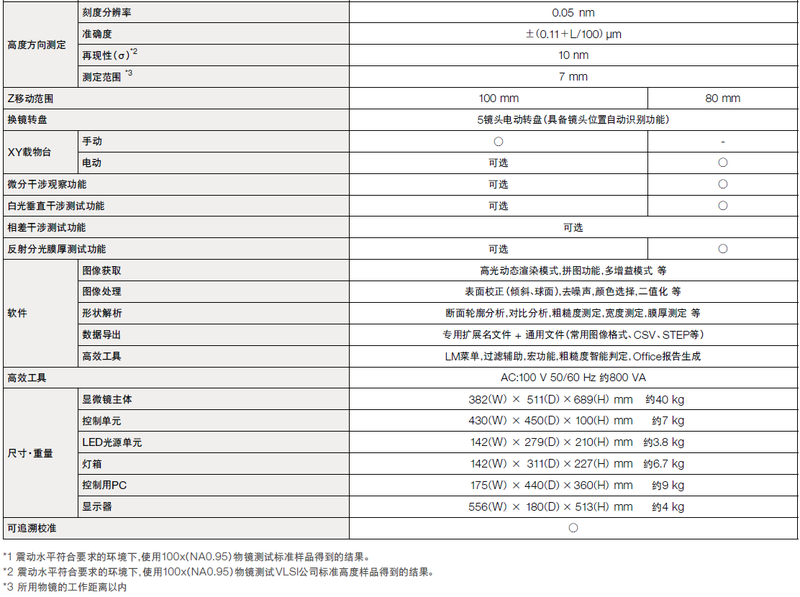
| Height Scale Resolution | 0.05 nm |
| Height Accuracy | ±(0.11+L/100) μm |
| Height Reproducibility [σ;100×(NA0.95) Objective and VLSI Company Standard Height Sample] | 10 nm |
| Height Measurement Range [Used Objective Working Distance Within] | 7 mm |
| Objective Turret | 5 Lens Motorized Turret , Provides Lens Position Automatic Recognition Function |
| Phase Contrast Interferometry test Function | Optional |
| Software Image Acquisition | High Dynamic Range Rendering mode 、 Image Stitching Function 、 Multiple Gain mode and Others |
| Software Image Processing | surface Calibration ( tilt 、 Spherical )、 Denoising 、 Color Selection 、 Binarization and Others |
| Software Shape Analysis | Cross Section Profile Analysis 、 Comparison Analysis 、 Roughness Measurement 、 width Measurement 、 Film Thickness Measurement and Others |
| Software Data Export | Proprietary and General Files ( Common Image Formats 、CSV、STEP and Others ) |
| Software Productivity Tools | LM Menu 、 Filtering Aid 、 Macro Function 、 Intelligent Roughness Assessment 、Office Report Generation |
| Power Supply parameter | AC100V 50/60Hz; Approximately 800VA |
| Microscope Body Dimensions and Weight | 382(W)×511(D)×689(H)mm; Approximately 40kg |
| Control Unit Dimensions and Weight | 430(W)×450(D)×100(H)mm; Approximately 7kg |
| LED Light Source Unit Dimensions and Weight | 142(W)×279(D)×210(H)mm; Approximately 3.8kg |
| Light Box Dimensions and Weight | 142(W)×311(D)×227(H)mm; Approximately 6.7kg |
| Control PC Dimensions and Weight | 175(W)×440(D)×360(H)mm; Approximately 9kg |
| Monitor Dimensions and Weight | 556(W)×180(D)×513(H)mm; Approximately 4kg |
| Z Travel Range | 100 mm |
| XY Sample Stage Manual Configuration | ○ |
| XY Sample Stage Motorized Configuration | Optional |
| Differential Interference Contrast Observation | Optional |
| Vertical White Light Interferometry test Function | Optional |
| Reflectometric Film Thickness Measurement | Optional |
Key Features
Datasheet
Please provide your email to download the datasheet.
Invalid email format. Please try again.
Supplier Information
Related Products
-
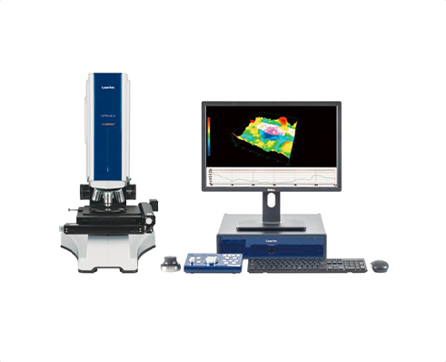 Laser and White Light Confocal Microscope L3
Microscopes
Oelectron
Zoom Magnification: 1×–8× Light Intensity Frame Storage: 1024×1024×12bit; High Definition mode 2048×2048×12bit Height Frame Storage: 1024×1024×16bit; High Definition mode 2048×2048×16bit
Lasertec, Japan, introduced the OPTELICS Hybrid confocal microscope, combining laser and white light sources for versatile, high performance confocal microscopy. Two sets of confocal optics work with accessories including an interferometer, differential interference contrast observation and spectral reflectance film thickness measurement. Lasertec is a Japanese semiconductor inspection equipment company founded in 1960, primarily supplying semiconductor wafer and photomask…
-
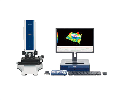 Laser and White Light Confocal Microscope L7
Microscopes
Oelectron
Zoom Magnification: 1×–8× Light Intensity Frame Storage: 1024×1024×12bit; High Definition mode 2048×2048×12bit Height Frame Storage: 1024×1024×16bit; High Definition mode 2048×2048×16bit
Lasertec, Japan, introduced the OPTELICS Hybrid confocal microscope, combining laser and white light sources for versatile, high performance confocal microscopy. Two sets of confocal optics work with accessories including an interferometer, differential interference contrast observation and spectral reflectance film thickness measurement. Lasertec is a Japanese semiconductor inspection equipment company founded in 1960, primarily supplying semiconductor wafer and photomask…
-
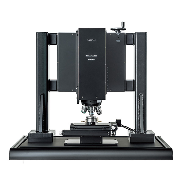 Confocal Electrochemical Reaction Visualization System
Microscopes
Oelectron
A true color confocal optical system receives only light reflected from the focal plane, the electrode active material surface. Glass surfaces and electrolyte therefore do not affect the observation, permitting high definition color images with strong color separation. Observation images are high definition true color images from the confocal system. Dedicated window cells are designed for in situ observation according to the application. The basic block fixture accommodates button electrodes; the advanced laminated cell model accommodates pouch cells. A dedicated temperature chamber holds block and laminated cells. Its interior remains dry to prevent condensation. Temperature control range: −30°C to 80°C.
-
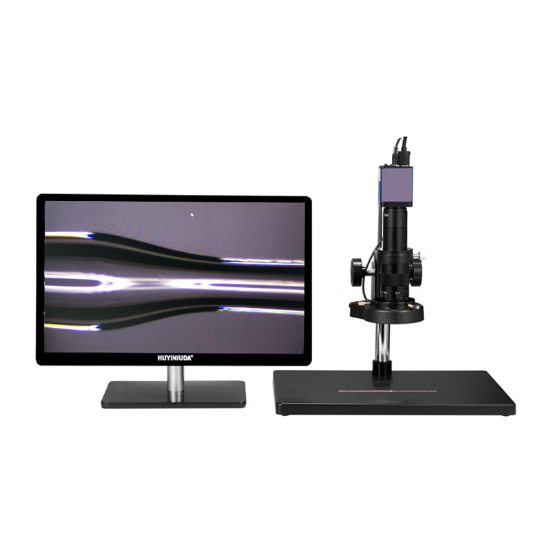 High Resolution CCD Measuring Microscope (XQ3210)
Microscopes
Szoscom
High Precision Measurement: ≥3u Pixel: 220 Ten Thousand Objective Magnification: 0.7X-4.5X Continuous Zoom
The XQ3210 high resolution CCD measuring microscope uses a 2 megapixel high speed HDMI camera with 1920×1080 resolution and 60 frames per second. It measures diameters of fibers, fiber bundles and glass tubes in line. Tools measure point spacing, point to line and line to line distances, angles, radians, parallel lines, horizontal and vertical parallel lines, circles, center to center and edge distances, point to center and line to center distances, polylines, rectangles and polygons. It is practical and easy to operate, with micrometer level accuracy.
Related Articles
Driven by the continuous pursuit of higher precision and efficiency in optical communication and optoelectronic device manufacturing, OLCR-1000 Low-Coherence Interferometer, independently developed by Wuhan Guanggu Interconnect Technology Co., Ltd., provides an innovative technical solution for distributed return loss testing of optical fibers and optoelectronic devices.
icrolight is a high-tech enterprise specializing in the R&D, manufacturing and sales of active and passive photonic devices for microwave photonics, LiDAR ranging, gas sensing, fiber optics and photomedicine.
BEIJING JIEPU TREND supplies YAG+Er:YAG+YAG bonded composite slab laser crystals for high‑power solid‑state laser systems. The monolithic slab consists of two undoped YAG end‑cap layers and a central Er‑doped YAG gain segment. The overall dimension is 9 mm×9 mm×9 mm.
Shanghai Connet Laser Technology Co., Ltd. focuses on technological innovation, delivering cutting-edge photonic products & solutions for industrial lasers, LiDAR, fiber optic sensing, coherent telecom, cold atom physics and precision spectroscopy research & mass manufacturing.
Loading...
Name
Phone
Organization
Use Case

Database Platform