
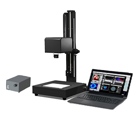
NIR Series Stress Birefringence Measurement System PA-300-NIR(850/940)
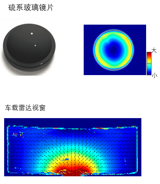
PA-300-NIR uses an 850nm near infrared measurement wavelength and 5 megapixel resolution to rapidly map birefringence and internal stress, including in materials opaque to the naked eye. It is suitable for chalcogenide glass that transmits near infrared light. WPA-200-NIR uses three near infrared measurement wavelengths to obtain birefringence information in near infrared transmitting products. It is suitable for stress birefringence measurement of automotive LiDAR components.
 Save to Favorites
Overview
Specifications
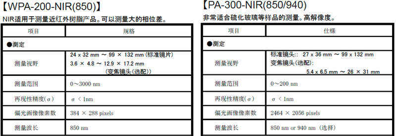
| Parameter | Value |
|---|---|
| Measurement Field of View [Standard Lens] | 27×36mm–99×132mm |
| Measurement Field of View [Optional Zoom Lens] | 5.4×6.5mm–26×31mm |
| Measurement Range | 0–200 nm |
| Reproducibility σ | <1 nm |
| Polarized Image Pixel Count | 2464 pixels × 2056 pixels |
| Measurement wavelength | 850nm or 940nm( Selection ) |
Key Features
Datasheet
Please provide your email to download the datasheet.
Invalid email format. Please try again.
Supplier Information
Related Products
-
FlaTester Flatness Measurement Instrument Family FT100 Optical Metrology Shineoptics
Structural Configuration: Inverted Measurement Method: Grazing incidence Light Source: Helium-neon laser (632.8nm)
In modern precision manufacturing, single-line scanners and coordinate measuring machines collect too little data to determine flatness over an entire surface. The FlaTester flatness instrument measures complete part surfaces without contact in seconds, accommodating different sizes and complex shapes. FlaTester has 5nm resolution and 50nm accuracy, enabling rapid, precise measurement of flatness, profile, radius, and other surface parameters across various materials and surface finishes.
-
Autocollimator Optical Metrology Jptoe
Objective Focal Length: 150 mm Objective Aperture [CA=90%]: 30mm(CA=90%) Detector: CMOS 3072 × 2048
An autocollimator measures very small angles with high precision using optical autocollimation. It provides noncontact, sensitive, stable, and convenient detection of angular deviation, straightness, and flatness for precision manufacturing, optical inspection, industrial metrology, and automation. A source illuminates a reticle;the objective collimates it into a parallel beam directed at the test reflector. Returning light retraces the path through the objective and forms an image on a precision sensor. Small reflector tilts displace the image;precise displacement detection and algorithms convert the shift to angular deviation, enabling subarcsecond measurements.
-
Saturated Absorption Assembly Optical Metrology Spectra-line
Operating Wavelength [Other wavelengths customizable]: 767nm/770nm/780nm/795nm..., other wavelengths can be customized Maximum Input Optical Power: <1mW Reference Cell Fill Material [Reference cells with other substances can be customized]: K/Rb/Cs; reference cells with other substances can be customized
Saturated-absorption stabilization module is a compact fiber-coupled reference for tunable diode/fiber lasers. Proprietary Puxian Technology design locks lasers to atomic hyperfine transitions for stable frequency. Components:baseplate,fiber collimator,λ/2 andλ/4 waveplates,mirrors,aperture,detector and reference cell.
-
Microcrystalline Reference Mirror Optical Metrology Sc-light
Specification Range [Processing capability; product name: Microcrystalline Standard Mirror]: D2-D650 Surface Figure [Processing capability; product name: Microcrystalline Standard Mirror; specification range: D2-D650 MM]: PV1/10 RMS [Processing capability; product name: Microcrystalline Standard Mirror; specification range: D2-D650 MM]: RMS 1/70
-
H-K9L Reference Mirror Optical Metrology Sc-light
Processing Capability - Specification Range: D2-D450 Processing Capability - Surface Figure: PV1/20 Processing Capability -RMS: RMS 1/100
Related Articles
Driven by the continuous pursuit of higher precision and efficiency in optical communication and optoelectronic device manufacturing, OLCR-1000 Low-Coherence Interferometer, independently developed by Wuhan Guanggu Interconnect Technology Co., Ltd., provides an innovative technical solution for distributed return loss testing of optical fibers and optoelectronic devices.
icrolight is a high-tech enterprise specializing in the R&D, manufacturing and sales of active and passive photonic devices for microwave photonics, LiDAR ranging, gas sensing, fiber optics and photomedicine.
BEIJING JIEPU TREND supplies YAG+Er:YAG+YAG bonded composite slab laser crystals for high‑power solid‑state laser systems. The monolithic slab consists of two undoped YAG end‑cap layers and a central Er‑doped YAG gain segment. The overall dimension is 9 mm×9 mm×9 mm.
Shanghai Connet Laser Technology Co., Ltd. focuses on technological innovation, delivering cutting-edge photonic products & solutions for industrial lasers, LiDAR, fiber optic sensing, coherent telecom, cold atom physics and precision spectroscopy research & mass manufacturing.
Loading...
Name
Phone
Organization
Use Case

Database Platform