
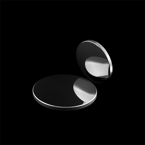
Silicon Aspheric Lens PAsSi-
Silicon aspherical lenses have advantages such as high transmittance, high precision, and high stability, and can be used to manufacture high-precision optical systems and instruments, such as infrared imaging systems, infrared spectrometer systems, etc. Due to its high refractive index and dispersion properties, silicon can also be used to manufacture lenses and lenses with special optical effects. It can be coated with MgF2, UV-AR, UV-VIS, VIS-EXT, VIS-NIR, NIR I, NIR II, Telecom NIR, SWIR, SWIR, YAG-BBAR and other film systems.
 Save to Favorites
Overview
Specifications
| Parameter | Value |
|---|---|
| Dia | 2-300 mm |
| Focal Length | 15-5000 mm |
| Center Thickness | 0.12-60 mm |
| Edge Thickness | 0.12-60 mm |
| Design Wavelength | Custom |
| Radius of Curvature | Custom |
| Surface Quality | 60-40 |
| Diameter Tolerance | +0.0/-0.1 |
| Thk Tolerance | ±0.1 mm |
| Substrate Material | Silicon(Si) |
| PV [@632.8nm] | λ/4 |
| Centering | <3′ |
| Clear Aperture | >90% |
| Coating | Uncoated |
| REACH | Compliant |
| ROHS | Compliant |
| Transmission Range [Substrate Material:Silicon(Si)] | 1.2-15μm |
| Refractive Index [Substrate Material:Silicon(Si);@10μm] | 3.41776%@10μm |
| Reflection Loss [Substrate Material:Silicon(Si);@10μm] | 46.1%@10μm |
| Structure [Substrate Material:Silicon(Si)] | Single crystal,synthetic |
| Cleavage Planes [Substrate Material:Silicon(Si)] | <111> |
| Density [Substrate Material:Silicon(Si)] | 2.33 g/cm³ |
| Melting Point [Substrate Material:Silicon(Si)] | 1414 ℃ |
| Thermal Conductivity [Substrate Material:Silicon(Si);@313K] | 163 @ 313K |
| Thermal Expansion [Substrate Material:Silicon(Si);@293K] | 2.6 @ 293K |
| Knoop Hardness [Substrate Material:Silicon(Si)] | 1100 kg/mm² |
| Specific Heat Capacity [Substrate Material:Silicon(Si)] | 712.8 J/(kg×K) |
| Dielectric Constant [Substrate Material:Silicon(Si);@f= 9.37GHz] | 13 @f= 9.37GHz |
| Young's Modulus (E) [Substrate Material:Silicon(Si)] | 130.91 GPa |
| Shear Modulus(G) [Substrate Material:Silicon(Si)] | 79.92 GPa |
| Bulk Modulus(K) [Substrate Material:Silicon(Si)] | 101.97 GPa |
| Poisson Coefficient [Substrate Material:Silicon(Si)] | 0.266 |
| Solubility [Substrate Material:Silicon(Si)] | None |
| Molecular Weight [Substrate Material:Silicon(Si)] | 28.09 g/mol |
Applications
Datasheet
Please provide your email to download the datasheet.
Invalid email format. Please try again.
Supplier Information
Related Products
-
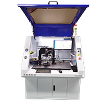 Tera3001-SA dual-LENS multidaughterboard coupling equipment
Optical Lenses
Terawan
The Tera3001-s multidaughterboard automatic alignment platform serves 10G/14G/25G optical transceivers. It mainly aligns lenses in Chip On Board (COB) modules, with single- or dual-channel lens/source alignment, automatic dispensing, and UV curing. The Tera3001-S provides high coupling efficiency, stability, and UPH depending on customer design, plus one-button collision protection and UV protection.
-
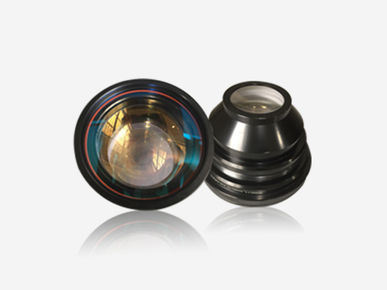 355 field lens
Optical Lenses
Central-laser
Focal Length [Original Table Row 2; Focal Length=100mm; Parallel Values in the Same Row Not Split into Separate Models or Configurations]: 100 mm Working Distance [Original Table Row 2; Focal Length=100mm; Parallel Values in the Same Row Not Split into Separate Models or Configurations]: 136 mm Scan Range [Original Table Row 2; Focal Length=100mm; Parallel Values in the Same Row Not Split into Separate Models or Configurations]: 70 mm² × 70 mm²
355 field lens: large zinc-selenide (ZnSe) focusing lens with a small spot for accurate marking. Imported lens material provides long service life and reduces removal, installation, and alignment. The 355nm scanning field lens is suitable for ultraviolet laser-marking machines.
-
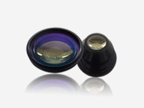 532 field lens
Optical Lenses
Central-laser
Focal Length [Original Table Row 2; Focal Length=100mm; Parallel Values in the Same Row Not Split into Separate Models or Configurations]: 100 mm Working Distance [Original Table Row 2; Focal Length=100mm; Parallel Values in the Same Row Not Split into Separate Models or Configurations]: 114.5 mm Scan Range [Original Table Row 2; Focal Length=100mm; Parallel Values in the Same Row Not Split into Separate Models or Configurations]: 70 mm² × 70 mm²
532 field lens: large zinc-selenide (ZnSe) focusing lens with a small spot for accurate marking. Imported lens material provides long service life and reduces removal, installation, and alignment. The 532nm field lens is suitable for green laser-marking machines.
-
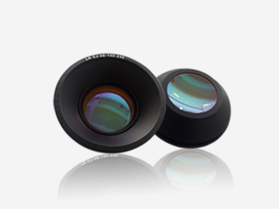 CO2 field lens
Optical Lenses
Central-laser
Focal Length [Original table row 2; Focal length=72mm; Parallel values in the same row, without additional model or configuration splitting]: 72 mm Mirror Diameter [Original table row 2; Focal length=72mm; Parallel values in the same row, without additional model or configuration splitting]: 48 mm Scan Range [Original table row 2; Focal length=72mm; Parallel values in the same row, without additional model or configuration splitting]: 50 mm² × 50 mm²
CO2 field lens: large zinc-selenide (ZnSe) focusing lens with a small spot for accurate marking. Imported lens material provides long service life and reduces removal, installation, and alignment. The 10640nm scanning field lens is suitable for CO2 laser-marking machines.
-
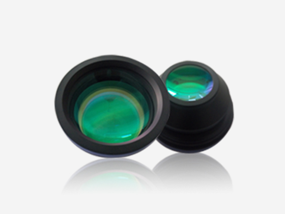 YAG field lens
Optical Lenses
Central-laser
Focal Length [Original table row 2; Focal length=63mm; Parallel values in the same row, without additional model or configuration splitting]: 63 mm Working Distance [Original table row 2; Focal length=63mm; Parallel values in the same row, without additional model or configuration splitting]: 78 mm Scan Range [Original table row 2; Focal length=63mm; Parallel values in the same row, without additional model or configuration splitting]: 50 mm² × 50 mm²
YAG field lens: large zinc-selenide (ZnSe) focusing lens with a small spot for accurate marking. Imported lens material provides long service life and reduces removal, installation, and alignment. The 1064nm scanning field lens is suitable for fiber laser-marking machines.
Related Articles
The petrochemical industry features continuous high-risk production, where production equipment operates uninterruptedly under extreme working conditions including high temperature, high pressure, strong corrosion and oxidation.
Driven by the continuous pursuit of higher precision and efficiency in optical communication and optoelectronic device manufacturing, OLCR-1000 Low-Coherence Interferometer, independently developed by Wuhan Guanggu Interconnect Technology Co., Ltd., provides an innovative technical solution for distributed return loss testing of optical fibers and optoelectronic devices.
Driven by the rapid upgrading of intelligent vehicles, optoelectronic sensing technologies represented by laser sensing and infrared thermal imaging have become core pillars for high-level autonomous driving and smart cockpit iteration. Leveraging automotive-grade optoelectronic R&D advantages, Pilot Technology Group launches the VITAL intelligent vehicle solution. By integrating high-power VCSEL laser chips and vehicle infrared night-vision thermal imagers, the system comprehensively enhances vehicle environmental perception and realizes safer, smarter and more comfortable driving experiences.
Fiber lasers and fiber amplification systems require excitation sources with stable wavelength, narrow spectral linewidth and consistent output power.
Loading...
Name
Phone
Organization
Use Case

Database Platform