

Zero-Astigmatism Imaging Spectrometer HELENA
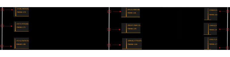
Ideaoptics' HELENA zero-astigmatism imaging spectrograph uses a unique astigmatism-correcting optical design to eliminate conventional-instrument astigmatism and provide uniform, sharp spectral images across the focal plane. Its0.08nm spectral resolution and suppression of multichannel crosstalk improve weak-signal detection and the purity and reliability of multichannel spectral analysis. It supports advanced research in single-molecule fluorescence, transient spectroscopy, and fine-structure analysis of nanomaterials, providing a reliable tool for precision spectroscopy.
 Save to Favorites
Overview
Specifications
| Parameter | Value |
|---|---|
| Focal Length [Unless Otherwise Stated, All Specifications Were Measured Using a 1200 g/mm Grating at 435.8nm.] | 320mm |
| Relative Aperture [Unless Otherwise Stated, All Specifications Were Measured Using a 1200 g/mm Grating at 435.8nm.] | f/4.6 |
| Spectral Resolution ‑PMT [Resolution Measurement Conditions:1200 grooves/mm Grating,546nm Wavelength,10-Micrometer Slit Width.] | 0.05 nm (10μm Slit ) |
| Spectral Resolution ‑CCD [Resolution Measurement Conditions:At Focal-Plane Center, Using a 10-Micrometer Slit and a Detector with 15um Pixels, Measured at 546nm.] | 0.08 nm |
| Reciprocal Linear Dispersion [Unless Otherwise Stated, All Specifications Were Measured Using a 1200 g/mm Grating at 435.8nm.] | 2.3 nm/mm |
| Wavelength Coverage(30-Millimeter-Wide CCD) [Unless Otherwise Stated, All Specifications Were Measured Using a 1200 g/mm Grating at 435.8nm.] | 63 nm |
| Focal Plane Dimensions(Width × Height) [Unless Otherwise Stated, All Specifications Were Measured Using a 1200 g/mm Grating at 435.8nm.] | 27mm × 22mm |
| Scanning Wavelength Range [Unless Otherwise Stated, All Specifications Were Measured Using a 1200 g/mm Grating at 435.8nm.] | 0‑1400 nm |
| Scan Step Size [Unless Otherwise Stated, All Specifications Were Measured Using a 1200 g/mm Grating at 435.8nm.] | 0.002 nm/step |
| Wavelength Accuracy [Unless Otherwise Stated, All Specifications Were Measured Using a 1200 g/mm Grating at 435.8nm.] | ±0.2 nm (up to ±0.02 nm after wavelength calibration) |
| Wavelength Repeatability [Unless Otherwise Stated, All Specifications Were Measured Using a 1200 g/mm Grating at 435.8nm.] | ±0.02 nm |
| Grating Turret [Unless Otherwise Stated, All Specifications Were Measured Using a 1200 g/mm Grating at 435.8nm.] | 1 (Accommodates 3 Gratings) |
| Number of Supported Turrets [Unless Otherwise Stated, All Specifications Were Measured Using a 1200 g/mm Grating at 435.8nm.] | 3;Interchangeable Triple-Grating Turret Module;Automatic System Calibration after Installation |
| Grating Switching Repeatability [Unless Otherwise Stated, All Specifications Were Measured Using a 1200 g/mm Grating at 435.8nm.] | 0.02 nm |
| Grating Dimensions [Unless Otherwise Stated, All Specifications Were Measured Using a 1200 g/mm Grating at 435.8nm.] | 68mm × 68mm |
| Astigmatism [Unless Otherwise Stated, All Specifications Were Measured Using a 1200 g/mm Grating at 435.8nm.] | Zero Astigmatism across All Wavelengths |
| Hardware Connection Ports [Unless Otherwise Stated, All Specifications Were Measured Using a 1200 g/mm Grating at 435.8nm.] | USB and RS‑232 |
| Development Library [Unless Otherwise Stated, All Specifications Were Measured Using a 1200 g/mm Grating at 435.8nm.] | C#、LABVIEW、Python |
| Certification [Unless Otherwise Stated, All Specifications Were Measured Using a 1200 g/mm Grating at 435.8nm.] | CE(EMC) |
| Overall Dimensions(Length × Width × Height) [Unless Otherwise Stated, All Specifications Were Measured Using a 1200 g/mm Grating at 435.8nm.] | 440mm×355mm×215mm(Excluding Accessories and Feet) |
| Optical Axis Height [Unless Otherwise Stated, All Specifications Were Measured Using a 1200 g/mm Grating at 435.8nm.] | 160mm‑186mm |
| Weight [Unless Otherwise Stated, All Specifications Were Measured Using a 1200 g/mm Grating at 435.8nm.] | 25.5kg |
| Operating Temperature / Humidity [Unless Otherwise Stated, All Specifications Were Measured Using a 1200 g/mm Grating at 435.8nm.] | Operating Temperature :5℃ ~30℃; Storage Temperature :‑10℃ ~50℃; Humidity :<50%( Relative humidity ) |
Applications
Key Features
Datasheet
Supplier Information
Related Products
-
Online In-Situ Fluorescence Spectrometer InView-PL Spectrometers Ideaoptics
Fluorescence Spectra [450nm Excitation ; Customizable]: 450nm Excitation,600~1100nm Fluorescence Detection Band(Customizable) Absorption Spectrum: 400~1100nm Spectral Resolution(Cooled): ~5nm
InView-PL is an online, in-situ fluorescence spectrometer for monitoring photovoltaic thin-film formation. It can be integrated with spin-coating, VCD, annealing, and film-aging equipment to monitor PL, absorption, and scattering signals in real time during film formation, crystallization, and aging. This helps researchers understand crystallization rates and phase-transition dynamics, optimize conditions, control crystallization, improve crystal quality, and increase device efficiency and stability.
-
Agilent CARY5000 Spectrometers DCGD
-
Agilent CARY7000 Spectrometers DCGD
-
HP-3010 200-1100nm Low-Noise Miniature Fiber Spectrometer Spectrometers Hhitgroup
Detector - Detector Type: Linear Array (CMOS) Detector - Effective Pixels: 2048 Detector - Pixel Size: 14μmx 200μm
The HP-3010 miniature spectrometer is a new low-noise miniature fiber spectrometer developed by Hhitgroup. The HY-3010 uses a high-sensitivity CMOS linear-array sensor covering the 200-1100nm wavelength range, with high sensitivity and extremely low noise. Applications include geographic spectral-data acquisition, water reflectance acquisition, transmission and reflection, spectral absorption, atomic emission spectroscopy, irradiance, absorbance, and color measurement. The HP-3010 fiber spectrometer uses a thoroughly optimized crossed asymmetric C-T optical path for high spectral resolution. Its distinctive stray-light suppression and low-noise circuit design provide excellent noise control, making it ideal for ultraviolet, visible, and near-infrared spectroscopy. The HP-3010 fiber spectrometer is compact, highly consistent, stable, and reliable. Wavelength range and optical resolution can be customized, and multiple trigger modes and secondary development support flexible application expansion.
-
Ultrabroadband Scanning Ti:Sapphire Laser Spectrometers Spectra-line
Wavelength range: 275-1100nm Wavelength range: (275-350 nm/350-550 nm/550-700 nm/700-1100 nm) Linewidth [depends on spectral range]: 1-6 GHz(depends on spectral range)
The fully automatic narrow-linewidth (<1GHz), ultrawide continuous-tuning system originates from intelligent tunable spectroscopy in nanotechnology. Advanced laser-component design combines Ti:sapphire and dye lasers with intracavity doubling for 275nm-1100nm coverage. Puxian Technology supplies Tekhnoscan-customized systems for spectral calibration, laser spectroscopy, and materials-science research.
Related Articles
Driven by the continuous pursuit of higher precision and efficiency in optical communication and optoelectronic device manufacturing, OLCR-1000 Low-Coherence Interferometer, independently developed by Wuhan Guanggu Interconnect Technology Co., Ltd., provides an innovative technical solution for distributed return loss testing of optical fibers and optoelectronic devices.
icrolight is a high-tech enterprise specializing in the R&D, manufacturing and sales of active and passive photonic devices for microwave photonics, LiDAR ranging, gas sensing, fiber optics and photomedicine.
BEIJING JIEPU TREND supplies YAG+Er:YAG+YAG bonded composite slab laser crystals for high‑power solid‑state laser systems. The monolithic slab consists of two undoped YAG end‑cap layers and a central Er‑doped YAG gain segment. The overall dimension is 9 mm×9 mm×9 mm.
Shanghai Connet Laser Technology Co., Ltd. focuses on technological innovation, delivering cutting-edge photonic products & solutions for industrial lasers, LiDAR, fiber optic sensing, coherent telecom, cold atom physics and precision spectroscopy research & mass manufacturing.
Loading...
Name
Phone
Organization
Use Case

Database Platform