

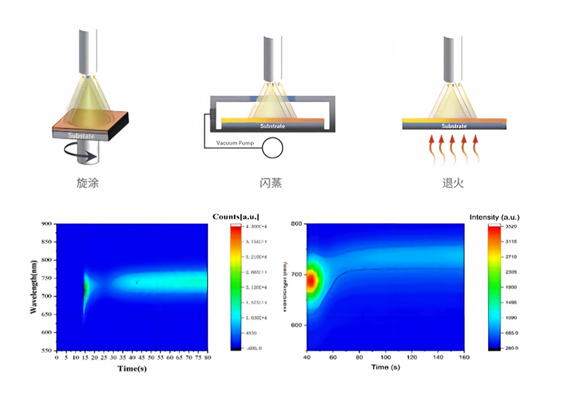
Online In-Situ Fluorescence Spectrometer InView-PL
InView-PL is an online, in-situ fluorescence spectrometer for monitoring photovoltaic thin-film formation. It can be integrated with spin-coating, VCD, annealing, and film-aging equipment to monitor PL, absorption, and scattering signals in real time during film formation, crystallization, and aging. This helps researchers understand crystallization rates and phase-transition dynamics, optimize conditions, control crystallization, improve crystal quality, and increase device efficiency and stability.
 Save to Favorites
Overview
Specifications
| Parameter | Value |
|---|---|
| Fluorescence Spectra [450nm Excitation ; Customizable] | 450nm Excitation,600~1100nm Fluorescence Detection Band(Customizable) |
| Absorption Spectrum | 400~1100nm |
| Spectral Resolution(Cooled) | ~5nm |
| Spectral Resolution(Uncooled) | ~10nm |
| Spot Size | φ3mm |
| Excitation Intensity | 0~0.1Suns 可调 |
| Working Distance | ≥10cm |
| Operating-Condition Sampling Rate | ≥10Hz |
| Accessories | Custom Brackets for Spin Coaters, Flash Evaporators, and Annealing Hotplates;Optional High-Throughput Measurement Accessories |
| Software | Supports Time-Sequence Fluorescence, Absorption, and Scattering Spectral Acquisition, and External Triggering |
Applications
Key Features
Datasheet
Supplier Information
Related Products
-
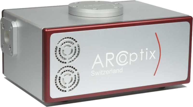 ARCoptix FT-MIR Rocket Fourier Transform Infrared Spectrometer FTMIR-L1-060-4TE
Spectrometers
Uniqueray
Beamsplitter Materials: CaF2 Measuring spectroscopy ranges ( Waves cm-1): 5000~1660 Measuring spectroscopy ranges ( Wavelength μm): 2~6
Switzerland ARCoptix Company production FT-IR“Rocket” Compact Fourier Transform Infrared Spectrometer ( Medium Infrared Spectrometer ) It's strong. 、 Small 、 Light and high performance properties 。FT-IR“Rocket” Available Optical Fiber Connection ( Here. Optical Fiber Inspect on-line in situ testing ), or free space measurements 。 Because of the use of photovoltaics Semiconductor Refrigeration MCT Mercury oxide detector ,FT-IR“Rocket” It provides high resolution and sensitivity. , Inline permanent alignment Interferometer and solid reference Laser Ensure high performance at each scan 。 The system is in Wavelength And it's very stable on the scale of the signal. , is Ideal tools for high-recurrence chemical measurements analysis 。 The system is also... is An optical spectrum analyser (OSA), Available for measurement Infrared Laser ,LED Spectra information for the same light source 。
-
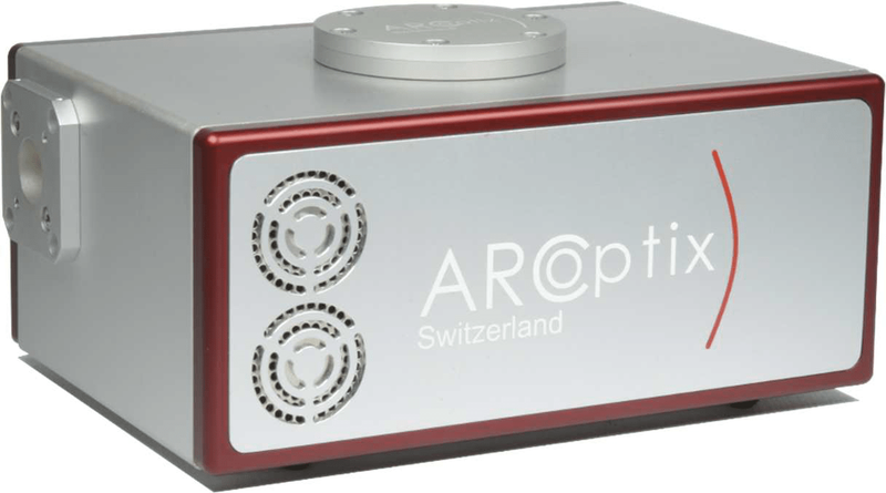 ARCoptix FT-MIR Rocket Fourier Transform Infrared Spectrometer FTMIR-L1-085-4TE
Spectrometers
Uniqueray
Beamsplitter Materials: CaF2 Measuring spectroscopy ranges ( Waves cm-1): 6600~1200 Measuring spectroscopy ranges ( Wavelength μm): 1.5~8.5
Switzerland ARCoptix Company production FT-IR“Rocket” Compact Fourier Transform Infrared Spectrometer ( Medium Infrared Spectrometer ) It's strong. 、 Small 、 Light and high performance properties 。FT-IR“Rocket” Available Optical Fiber Connection ( Here. Optical Fiber Inspect on-line in situ testing ), or free space measurements 。 Because of the use of photovoltaics Semiconductor Refrigeration MCT Mercury oxide detector ,FT-IR“Rocket” It provides high resolution and sensitivity. , Inline permanent alignment Interferometer and solid reference Laser Ensure high performance at each scan 。 The system is in Wavelength And it's very stable on the scale of the signal. , is Ideal tools for high-recurrence chemical measurements analysis 。 The system is also... is An optical spectrum analyser (OSA), Available for measurement Infrared Laser ,LED Spectra information for the same light source 。
-
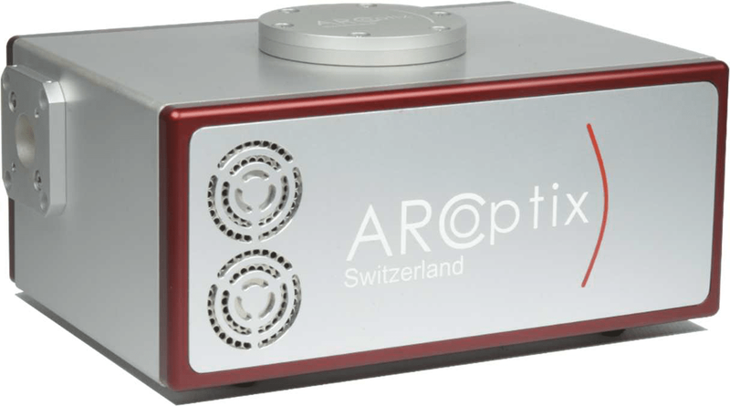 ARCoptix FT-MIR Rocket Fourier Transform Infrared Spectrometer FTMIR-L1-120-4TE
Spectrometers
Uniqueray
Beamsplitter Materials: ZnSe Measuring spectroscopy ranges ( Waves cm-1): 5000~830 Measuring spectroscopy ranges ( Wavelength μm): 2~12
Switzerland ARCoptix Company production FT-IR“Rocket” Compact Fourier Transform Infrared Spectrometer ( Medium Infrared Spectrometer ) It's strong. 、 Small 、 Light and high performance properties 。FT-IR“Rocket” Available Optical Fiber Connection ( Here. Optical Fiber Inspect on-line in situ testing ), or free space measurements 。 Because of the use of photovoltaics Semiconductor Refrigeration MCT Mercury oxide detector ,FT-IR“Rocket” It provides high resolution and sensitivity. , Inline permanent alignment Interferometer and solid reference Laser Ensure high performance at each scan 。 The system is in Wavelength And it's very stable on the scale of the signal. , is Ideal tools for high-recurrence chemical measurements analysis 。 The system is also... is An optical spectrum analyser (OSA), Available for measurement Infrared Laser ,LED Spectra information for the same light source 。
-
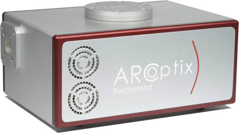 ARCoptix FT-MIR Rocket Fourier Transform Infrared Spectrometer FTMIR-L1-160- LN2
Spectrometers
Uniqueray
Beamsplitter Materials: ZnSe Measuring spectroscopy ranges ( Waves cm-1): 5000~650 Measuring spectroscopy ranges ( Wavelength μm): 2~16
Switzerland ARCoptix Company production FT-IR“Rocket” Compact Fourier Transform Infrared Spectrometer ( Medium Infrared Spectrometer ) It's strong. 、 Small 、 Light and high performance properties 。FT-IR“Rocket” Available Optical Fiber Connection ( Here. Optical Fiber Inspect on-line in situ testing ), or free space measurements 。 Because of the use of photovoltaics Semiconductor Refrigeration MCT Mercury oxide detector ,FT-IR“Rocket” It provides high resolution and sensitivity. , Inline permanent alignment Interferometer and solid reference Laser Ensure high performance at each scan 。 The system is in Wavelength And it's very stable on the scale of the signal. , is Ideal tools for high-recurrence chemical measurements analysis 。 The system is also... is An optical spectrum analyser (OSA), Available for measurement Infrared Laser ,LED Spectra information for the same light source 。
-
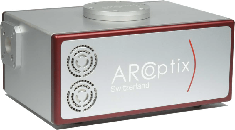 ARCoptix FT-MIR Rocket Fourier Transform Infrared Spectrometer FTMIR-L1-160- DLA
Spectrometers
Uniqueray
Beamsplitter Materials: ZnSe Measuring spectroscopy ranges ( Waves cm-1): 5000~650 Measuring spectroscopy ranges ( Wavelength μm): 2~16
Switzerland ARCoptix Company production FT-IR“Rocket” Compact Fourier Transform Infrared Spectrometer ( Medium Infrared Spectrometer ) It's strong. 、 Small 、 Light and high performance properties 。FT-IR“Rocket” Available Optical Fiber Connection ( Here. Optical Fiber Inspect on-line in situ testing ), or free space measurements 。 Because of the use of photovoltaics Semiconductor Refrigeration MCT Mercury oxide detector ,FT-IR“Rocket” It provides high resolution and sensitivity. , Inline permanent alignment Interferometer and solid reference Laser Ensure high performance at each scan 。 The system is in Wavelength And it's very stable on the scale of the signal. , is Ideal tools for high-recurrence chemical measurements analysis 。 The system is also... is An optical spectrum analyser (OSA), Available for measurement Infrared Laser ,LED Spectra information for the same light source 。
Related Articles
Driven by the continuous pursuit of higher precision and efficiency in optical communication and optoelectronic device manufacturing, OLCR-1000 Low-Coherence Interferometer, independently developed by Wuhan Guanggu Interconnect Technology Co., Ltd., provides an innovative technical solution for distributed return loss testing of optical fibers and optoelectronic devices.
icrolight is a high-tech enterprise specializing in the R&D, manufacturing and sales of active and passive photonic devices for microwave photonics, LiDAR ranging, gas sensing, fiber optics and photomedicine.
BEIJING JIEPU TREND supplies YAG+Er:YAG+YAG bonded composite slab laser crystals for high‑power solid‑state laser systems. The monolithic slab consists of two undoped YAG end‑cap layers and a central Er‑doped YAG gain segment. The overall dimension is 9 mm×9 mm×9 mm.
Shanghai Connet Laser Technology Co., Ltd. focuses on technological innovation, delivering cutting-edge photonic products & solutions for industrial lasers, LiDAR, fiber optic sensing, coherent telecom, cold atom physics and precision spectroscopy research & mass manufacturing.
Loading...
Name
Phone
Organization
Use Case

Database Platform