

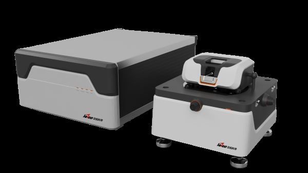
TopSPM-AD Atomic Force Microscope with Self-Sensing Probe
The product originated from the State Key Laboratory of Optoelectronic Materials and Technologies at Sun Yat-sen University. Its technology has reached the level of internationally advanced products, with research achievements overcoming international restrictions and technical barriers. The team maintains long-term collaborations with the Guangdong Integrated Circuit Engineering Technology Research Center, the Guangdong Green Power Conversion and Intelligent Control Engineering Technology Research Center, the School of Physics and the testing center at Sun Yat-sen University, other universities and research institutes, and leading domestic companies in related fields. Its expertise covers surface analysis, weak-signal detection, measurement and control system design, and instrument development and production.
 Save to Favorites
Overview
Specifications
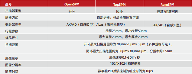
| Parameter | Value |
|---|---|
| Scanner Type | Closed Loop |
| Sample Introduction Method | Automatic Sample Introduction with Adjustable Sample Measurement Position |
| Probe Holder Type | AK/AD (Self-Sensing) / Las (Laser-Detected) |
| Travel | 23 mm |
| Minimum Step Size | 50 nm |
| Maximum Sample Diameter | 20 mm |
| Maximum Sample Thickness | 20 mm |
| Maximum Scan Range [Closed Loop] | Approximately 30×30×8 |
| Resolution [Closed Loop] | Approximately 1.5 |
| Imaging Rate | 0.1–30 lines/s |
| Image Resolution | 1024 physical pixels × 1024 physical pixels |
| Digital PID Feedback Control Response Time | 10 μs |
Applications
Key Features
Datasheet
Please provide your email to download the datasheet.
Invalid email format. Please try again.
Supplier Information
Related Products
-
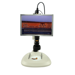 Integrated Video Microscope MIV90
Microscopes
Pomeas
Category [Lens]: Continuous-zoom lens Zoom-lens magnification [Lens]: 0.7X~4.5X (zoom ratio 6.5:1) Tube magnification [Lens]: 0.5 ×
The integrated video microscope can observe different components on PCB boards, focusing with simple adjustment for rapid observation, and can also observe LED chips. It can inspect the shapes of formed parts such as drills, turning tools, milling cutters, and dies, as well as syringe needles and other medical-device items.
-
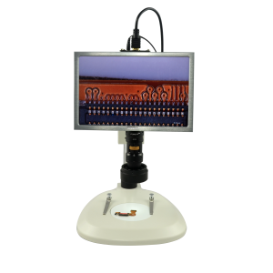 Integrated Video Microscope MIV90F
Microscopes
Pomeas
Category [Lens]: 12mm fine adjustment + coaxial Zoom-lens magnification [Lens]: 0.7X~4.5X (zoom ratio 6.5:1) Tube magnification [Lens]: 0.5 ×
The integrated video microscope can observe different components on PCB boards, focusing with simple adjustment for rapid observation, and can also observe LED chips. It can inspect the shapes of formed parts such as drills, turning tools, milling cutters, and dies, as well as syringe needles and other medical-device items.
-
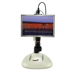 Integrated Video Microscope MIH90
Microscopes
Pomeas
Category [Lens]: Continuous-zoom lens Zoom-lens magnification [Lens]: 0.7X~4.5X (zoom ratio 6.5:1) Tube magnification [Lens]: 0.5 ×
The integrated video microscope can observe different components on PCB boards, focusing with simple adjustment for rapid observation, and can also observe LED chips. It can inspect the shapes of formed parts such as drills, turning tools, milling cutters, and dies, as well as syringe needles and other medical-device items.
-
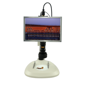 Integrated Video Microscope MIH90F
Microscopes
Pomeas
Category [Lens]: 12mm fine adjustment + coaxial Zoom-lens magnification [Lens]: 0.7X~4.5X (zoom ratio 6.5:1) Tube magnification [Lens]: 0.5 ×
The integrated video microscope can observe different components on PCB boards, focusing with simple adjustment for rapid observation, and can also observe LED chips. It can inspect the shapes of formed parts such as drills, turning tools, milling cutters, and dies, as well as syringe needles and other medical-device items.
-
Industrial microscope series
Microscopes
Intaneoptics
Numerical Aperture [Visible-light industrial apochromatic objective; M Plan Apo 2X; Specification table in parameter image 1]: 0.06 Working Distance WD [Visible-light industrial apochromatic objective; M Plan Apo 2X; Specification table in parameter image 1]: 34 mm Focal Length f [Visible-light industrial apochromatic objective; M Plan Apo 2X; Specification table in parameter image 1]: 100 mm
Related Articles
The petrochemical industry features continuous high-risk production, where production equipment operates uninterruptedly under extreme working conditions including high temperature, high pressure, strong corrosion and oxidation.
Driven by the continuous pursuit of higher precision and efficiency in optical communication and optoelectronic device manufacturing, OLCR-1000 Low-Coherence Interferometer, independently developed by Wuhan Guanggu Interconnect Technology Co., Ltd., provides an innovative technical solution for distributed return loss testing of optical fibers and optoelectronic devices.
Driven by the rapid upgrading of intelligent vehicles, optoelectronic sensing technologies represented by laser sensing and infrared thermal imaging have become core pillars for high-level autonomous driving and smart cockpit iteration. Leveraging automotive-grade optoelectronic R&D advantages, Pilot Technology Group launches the VITAL intelligent vehicle solution. By integrating high-power VCSEL laser chips and vehicle infrared night-vision thermal imagers, the system comprehensively enhances vehicle environmental perception and realizes safer, smarter and more comfortable driving experiences.
Fiber lasers and fiber amplification systems require excitation sources with stable wavelength, narrow spectral linewidth and consistent output power.
Loading...
Name
Phone
Organization
Use Case

Database Platform