

YLF+Nd:YLF+YLF
Our YLF+Nd:YLF+YLF bonded crystal is formed by bonding pure YLF to both ends of Nd:YLF, effectively improving the overall performance of Nd:YLF lasers. The thermal conductivity of Nd:YLF is 0,06 W/cm/°K@25°C; that of pure YLF is 14W/m/K@20℃ and 10.5W/m/K@100℃. Bonding both ends to form YLF+Nd:YLF+YLF improves the thermal behavior of Nd:YAG, reduces pump-induced thermal lensing, improves beam quality and laser output efficiency at 1047nm and 1053nm, increases output stability, and extends laser service life. Crylink uses surface-activated bonding, a low- or room-temperature bonding technology characterized by surface cleaning and surface activation. Before bonding, bombardment of the bonding surfaces by fast atoms or ion beams can effectively increase bond strength and enable high-quality bonding among inorganic materials, metals, and semiconductors. Compared with high-temperature thermal bonding, surface-activated bonding provides higher interfacial bond strength and better control of optical absorption loss and surface-figure changes. In thermal diffusion bonding, impurities on the surfaces cannot be removed and become trapped at the bonding interface. Surface-activated bonding can remove polishing residues, organic contamination, and surface oxide layers, break chemical bonds in the material, and increase activation energy. The YLF+Nd:YLF+YLF bonded crystals have high bond strength, low absorption loss at the interface (generally less than 20ppm), and little surface-figure change at the interface (surface figure after bonding <lamda/8). Available shapes include rods, slabs, waveguides, and sandwich structures. Various coatings can be provided on both ends, including AR@1040~1060nm on both end faces or S1:HR@1047/1053nm, S2:PR@1047/1053nm. YLF+Nd:YLF+YLF bonded crystals are widely used in mode-locked lasers, continuous-wave lasers, and materials processing.
 Save to Favorites
Overview
Specifications
| Parameter | Value |
|---|---|
| concentrations [Materials:Nd:YLF] | 0.1~3% |
| Structure [Materials:YLF / Structure;Nd:YLF:Rods/Slabs/Sandwich/Waveguide/ / Structure;YLF:Rods/Slabs/Sandwich/Waveguide/] | Rods/Slabs/Sandwich/Waveguide/ |
| Structure [Materials:Nd:YLF / Structure;YLF:Rods/Slabs/Sandwich/Waveguide/] | Rods/Slabs/Sandwich/Waveguide/ |
| Structure [Materials:YLF / Structure;YLF:Rods/Slabs/Sandwich/Waveguide/ / Structure;Nd:YLF:Rods/Slabs/Sandwich/Waveguide/] | Rods/Slabs/Sandwich/Waveguide/ |
| End-face Configuration [Materials:YLF / End-face Configuration;Nd:YLF:Flat/Convex/Wedge / End-face Configuration;YLF:Flat/Convex/Wedge] | Flat/Convex/Wedge |
| End-face Configuration [Materials:Nd:YLF / End-face Configuration;YLF:Flat/Convex/Wedge] | Flat/Convex/Wedge |
| End-face Configuration [Materials:YLF / End-face Configuration;YLF:Flat/Convex/Wedge / End-face Configuration;Nd:YLF:Flat/Convex/Wedge] | Flat/Convex/Wedge |
| Side Configuration [Materials:YLF / Side Configuration;Nd:YLF:Polish/Fine Ground / Side Configuration;YLF:Polish/Fine Ground] | Polish/Fine Ground |
| Side Configuration [Materials:Nd:YLF / Side Configuration;YLF:Polish/Fine Ground] | Polish/Fine Ground |
| Side Configuration [Materials:YLF / Side Configuration;YLF:Polish/Fine Ground / Side Configuration;Nd:YLF:Polish/Fine Ground] | Polish/Fine Ground |
| Coating available [Materials:YLF / Coating available;YLF:AR@1040~1060nm / @1040~1060nm] | AR@1040~1060nm |
| Coating available [Materials:YLF / Coating available;YLF:PR@1047/1053nm / @1047/1053nm] | HR@1047/1053nm |
| Coating available [Materials:YLF / Coating available;YLF:HR@1047/1053nm / @1047/1053nm] | PR@1047/1053nm |
Key Features
Datasheet
Supplier Information
Related Products
-
 Dia.100mm TeO2 boule
Optical Crystals
Xkpho
Chemical equation: TeO2 Density: 6 g/cm² Melting point: 733 ℃
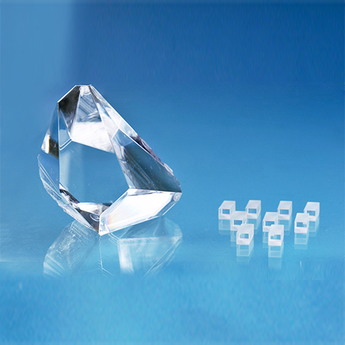
TeO2 is a kind of acousto-optic material with high quality factor. It has good properties of birefringence and optical rotation with low velocity of propagation along (110) axis.Under the same clear aperture, the acousto-optic device produced by TeO2 crystal has the advantages of the orders of magnitude improvement in resolution, fast response speed, small driving power, high diffraction efficiency, as well as stable and reliable performance. TeO2 crystal is an ideal single crystal material used to produce different kinds of acousto-optic device, such as acousto-optic deflector, modulator, resonator and tunable filter.
-
 LBO
Optical Crystals
Xkpho
Tolerance of cutting angle: △θ≤±0.25°,△φ≤±0.25° Tolerance of dimension: Dimension+/-0.1 mm,L:±0.1mm Flatness [@ 632.8nm]: λ/8 @ 632.8nm
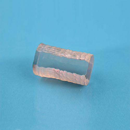
LBO crystals is an excellent nonlinear crystal.For frequency doubling(SHG),tripling(THG) of Nd:YAG,Nd:YLF,Nd:YVO4 lasers, it is one of the most useful nonlinear optical materials in ultraviolet and visible laser applications. LBO has the highest damage threshold in all the commonly-used inorganic NLO crystals. Therefore, it is the best candidate for high average power SHG and other nonlinear optical processes.
-
 TGG
Optical Crystals
Xkpho
Chemical Formula: Tb₃Ga₅O₁₂ Lattice Parameter a: a=12.355Å Growth Method: Czochralski
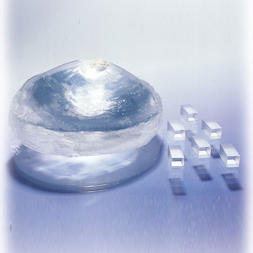
TGG is an excellent magneto-optical crystal used in various Faraday devices (Rotator and Isolator) in the range of 400nm-1100nm, excluding 475-500nm.
-
 Ultra thin BBO crystal wafer
Optical Crystals
Xkpho
Crystal Structure: Trigonal,Space Group R3c Lattice Parameter: a=b=12.532Å,c=12.717Å,Z=6 Melting Point: About 1095℃
BBO is a negative uniaxial crystal, with ordinary refractive index (No) larger than extraordinary refractive index (Ne). Both type I and type II phase matching can be reached by angle tuning. The phase matching angles of frequency doubling are shown in Fig. 2. Figure1. Transparency curve of BBO Figure2. SHG tuning curves of BBO The OPO and OPA of BBO are powerful tools for generating a widely tunable coherent radiation from UV to IR. The tuning angles of type I and type II BBO OPO and OPA have been calculated, with the results shown in Fig. 3 and Fig. 4, respectively. Figure 3. Type I OPO tuning curves of BBO Figure 4. Type II OPO tuning curves of BBO 1. OPO pumped at 532 nm An OPO output ranging from 680 nm to 2400 nm with the peak power of 1.6MW and up to 30% energy conversion efficiency was obtained in a 7.2 mm long type I BBO. The input pump energy was 40 mJ at 532 nm with pulse-width 75ps. With a longer crystal, higher conversion efficiency is expected. 2. OPO and OPA pumped at 355 nm In the case of Nd:YAG pumping, BBO's OPOs can generate more than 100mJ, with wavelength tunable from 400nm to 2000nm. Using XKPHO's BBO crystal, the OPO system covers a tuning range from 400nm to 3100nm which guarantees a maximum of 30% and more than 18% conversion efficiency, over the wavelength range from 430nm to 2000nm. Type II BBO can be used to decrease linewidth near the degenerate points. A linewidth as narrow as 0.05 nm and usable conversion efficiency of 12% were obtained. However, a longer (> 15mm) BBO should normally be used to decrease the oscillation threshold when employing the type II phase-matching scheme. Pumping with a picosecond Nd:YAG at 355 nm, a narrow-band (< 0.3 nm), high energy (> 200μJ) and wide tunable (400 nm to 2000 nm) pulse has been produced by BBO's OPAs. This OPA can reach as high as more than 50% conversion efficiency, and therefore is superior to common Dye lasers in many respects, including efficiency, tunable range, maintenance, and easiness in design and operation. Furthermore, coherent radiation from 205 nm to 3500 nm can be also generated by BBO's OPO or OPA plus a BBO for SHG. 3. Others A tunable OPO with signal wavelengths between 422nm and 477nm has been generated by angle tuning in a type ⅠBBO crystal pumped with a XeCl excimer laser at 308 nm. And a BBO's OPO pumped by the fourth harmonic of a Nd:YAG laser (at 266 nm) has been observed to cover the whole range of output wavelengths 330 nm - 1370 nm. When pumped by a 1mJ, 80 fs Dye laser at 615 nm, the OPA with two BBO crystals yields more than 50μJ (maximum 130 μJ), < 200 fs ultrashort pulse, over 800 nm - 2000 nm.
-
 BBO Crystal Basic characteristics
Optical Crystals
Iloptik
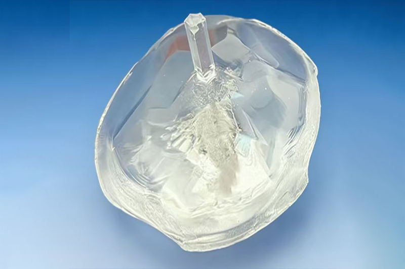
Basic Properties - Crystal Structure [Negative Uniaxial Crystal]: Trigonal Crystal System Basic Properties - Unit Cell Parameters [Room temperature]: a=b=12.532 Å,c=12.717 Å,Z=6 Basic Properties-Melting Point: 1095±5 ℃
BBO, β-barium borate crystal (β-Barium Borate Crystal), is an important nonlinear optical crystal widely used in laser technology and one of the most established nonlinear optical crystals for the ultraviolet band.
Related Articles
Electro-optic deflectors (EODs) are optical devices used to steer or deflect light beams by applying an electric field to a specialized optical crystal. Unlike mechanical beam steering systems that rely on moving mirrors, electro-optic deflectors enable high-speed, non-mechanical beam control with exceptional precision and responsiveness. They are widely used in laser scanning, optical communications, microscopy, laser printing, spectroscopy, and scientific research, where rapid and accurate laser beam positioning is essential.
The 850 nm and 940 nm infrared narrow‑bandpass filters launched by Innovation Photoelectric are core optical components specially designed for day‑and‑night security cameras. They effectively eliminate image interference during visible‑light and infrared‑illumination switching, delivering stable round‑the‑clock monitoring performance.
Within cutting‑edge ultrafast photonics research, asynchronous optical sampling (ASOPS) and synchronous sampling serve as fundamental technologies for terahertz excitation detection, coherent Raman imaging and other time‑resolved spectroscopy experiments.
Shanghai Connet Laser Technology Co., Ltd. focuses on technological innovation, delivering cutting-edge photonic products & solutions for industrial lasers, LiDAR, fiber optic sensing, coherent telecom, cold atom physics and precision spectroscopy research & mass manufacturing.
Loading...
Name
Phone
Organization
Use Case

Database Platform