

Nd:YVO₄+KTP
Our Nd:YVO₄+KTP bonded crystal is formed by bonding KTP to one end of Nd:YVO₄, effectively improving the overall performance of Nd:YVO₄ lasers. The thermal conductivity of Nd:YVO₄ is ∥C:5.23W/m/K and ⊥C:5.10W/m/K; that of KTP is 0.13W/m/k (@100℃). Bonding both ends to form Nd:YVO4+KTP improves the thermal behavior of Nd:YVO₄, reduces pump-induced thermal lensing, improves beam quality and laser output efficiency at 457nm and 671nm, increases output stability, and extends laser service life. Crylink uses surface-activated bonding, a low- or room-temperature bonding technology characterized by surface cleaning and surface activation. Before bonding, bombardment of the bonding surfaces by fast atoms or ion beams can effectively increase bond strength and enable high-quality bonding among inorganic materials, metals, and semiconductors. Compared with high-temperature thermal bonding, surface-activated bonding provides higher interfacial bond strength and better control of optical absorption loss and surface-figure changes. In thermal diffusion bonding, impurities on the surfaces cannot be removed and become trapped at the bonding interface. Surface-activated bonding can remove polishing residues, organic contamination, and surface oxide layers, break chemical bonds in the material, and increase activation energy. The Nd:YVO₄+KTP bonded crystals have high bond strength, low absorption loss at the interface (generally less than 20ppm), and little surface-figure change at the interface (surface figure after bonding <lamda/8). Available shapes include rods, slabs, waveguides, and sandwich structures. Various coatings can be provided on both ends, including AR@1064nm&532nm on both end faces. Nd:YVO₄+KTP bonded crystals are widely used in machinery, materials processing, spectroscopy, wafer inspection, displays, medical testing, laser printing, and data storage.
 Save to Favorites
Overview
Specifications
| Parameter | Value |
|---|---|
| concentrations [Materials:Nd:YVO₄] | 0.5%,1%, 2%,2,5%, 3% |
| Structure [Materials:Nd:YVO₄ / Structure;KTP:Rods/Slabs/Sandwich/Waveguide/] | Rods/Slabs/Sandwich/Waveguide/ |
| Structure [Materials:KTP / Structure;Nd:YVO₄:Rods/Slabs/Sandwich/Waveguide/] | Rods/Slabs/Sandwich/Waveguide/ |
| End-face Configuration [Materials:Nd:YVO₄ / End-face Configuration;KTP:Flat/Convex/Wedge] | Flat/Convex/Wedge |
| End-face Configuration [Materials:KTP / End-face Configuration;Nd:YVO₄:Flat/Convex/Wedge] | Flat/Convex/Wedge |
| Side Configuration [Materials:Nd:YVO₄ / Side Configuration;KTP:Polish/Fine Ground] | Polish/Fine Ground |
| Side Configuration [Materials:KTP / Side Configuration;Nd:YVO₄:Polish/Fine Ground] | Polish/Fine Ground |
| Coating available [Materials:Nd:YVO₄ / Coating available;KTP:AR@1064nm&532nm / @1064nm&532nm] | AR@1064nm&532nm |
| Coating available [Materials:KTP / Coating available;Nd:YVO₄:AR@1064nm&532nm / @1064nm&532nm] | AR@1064nm&532nm |
Key Features
Datasheet
Supplier Information
Related Products
-
 Er:Yb:Glass+Co:spinel
Laser Crystals
Xkpho
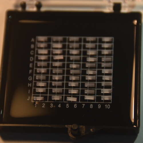
Material: Er:Yb:Glass+Co:MgAl2O4 Dimension: 0.9 mm × 0.9 mm × 3.7 mm Pumping: 915-955nm
-
 Nd:YAG
Laser Crystals
Xkpho
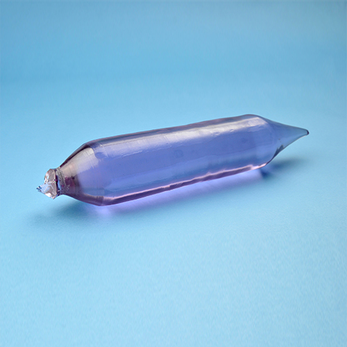
Doping: 0.1% ~ 2.5% Orientation: <111> , <100>,<110> crystalline direction Wavefront Distortion [@ 632.8 nm; per inch]: λ/10 per inch @ 632.8 nm
Nd:YAG is the earliest and most famous laser host crystal. Since it combines great advantages in many basic properties, Nd:YAG is the ubiquitous presence for near-infrared solid-state lasers and their frequency-doubler, tripler, and higher order multiplier. Slabs, thread rod, Er:YAG, Yb:YAG,Cr:YAG,Ce:YAG,Tm:YAG,Ho:YAG and other ion doped YAG crystals are also available upon request.
-
 Nd:YVO4
Laser Crystals
Xkpho
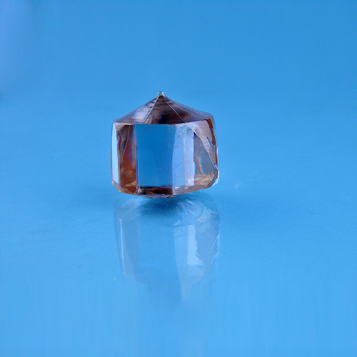
Atomic Density [Nd1.0%]: 1.26x10²⁰ atoms/cm3 (Nd1.0%) Crystal Structure: Zircon Tetragonal, space group D4h-I4/amd a=b=7.1193A,c=6.2892A Density: 4.22g/cm3
Nd:YVO4 is one of the most promising commercially available diode pumped solid state laser materials. It has high laser induced damage threshold and good mechanical in addition to optical properties. Its large stimulated emission cross-section and high absorption of pump laser make it a right crystal for pocket laser. Nd: YVO4 can produce IR green and blue laser by using minor different set-up. A broad absorption band centered at 808nm and favorable mechanical properties make Nd:YVO4 well suited for compact, efficient, high power diode-pumped lasers. Natural birefringence gives rise to a highly polarized output at 1064.3 and 1342nm.
-
 CLBO Crystal Basic characteristics
Laser Crystals
Iloptik
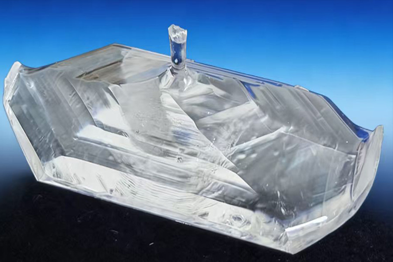
Basic Properties - Crystal Structure: Tetragonal Crystal System Basic Properties - Unit Cell Parameters [Room temperature]: a = b = 10.494 Å,c = 8.939 Å(1 Å = 10⁻¹⁰m) Basic Properties-Symmetry: Z=4
CLBO, or cesium lithium borate crystal (CsLiB₆O₁₀), is a high-performance new nonlinear optical crystal. Its broad transmission range, high nonlinear coefficient, wide spectral and temperature acceptance bandwidths, and absence of second-harmonic absorption make it outstanding for high-power laser frequency conversion and deep-ultraviolet generation.
-
 CLBO Crystal CLBO Crystal Specifications
Laser Crystals
Iloptik
CLBO Crystal Specifications - Dimensional Tolerance: (W±0.1mm)×(H±0.1mm)×(L+0.5/-0.1mm), Reception Custom CLBO Crystal Specifications - Effective Clear Aperture: 90% of the Central-Region Diameter CLBO Crystal Specifications - Surface Flatness [@ 633 nm]: λ/6 @ 633 nm
CLBO, or cesium lithium borate crystal (CsLiB₆O₁₀), is a high-performance new nonlinear optical crystal. Its broad transmission range, high nonlinear coefficient, wide spectral and temperature acceptance bandwidths, and absence of second-harmonic absorption make it outstanding for high-power laser frequency conversion and deep-ultraviolet generation.
Related Articles
As a core precision optical component for wavelength screening, frequency locking and spectral demodulation, optical etalons are widely used in high-end scientific research and precision laser equipment.
As a vital emerging sector of modern three-dimensional spatial economy, the low-altitude economy has become a new global growth driver. It covers a wide range of commercial scenarios, including UAV navigation and obstacle avoidance, precise airspace management, aerial mapping, low-altitude logistics distribution, security monitoring and emergency disaster rescue. Nevertheless, frequent extreme weather, complex terrain obstacles and increasingly dense low-altitude flight activities pose severe challenges to the safety and stability of low-altitude aircraft operations.
Laser pump sources are the core energy input component of solid-state lasers and laser amplifiers, and their performance directly determines the output power, beam quality and service life of the entire laser system. In scenarios such as industrial processing, scientific research experiments and high-end equipment, improper pump source selection will not only result in substandard system performance, but also bring a series of problems such as rapid device degradation and high operation and maintenance costs. This article sorts out the core selection logic and key pitfalls of pump source procurement, and provides selection references based on mature, mass-produced high-reliability products to help purchasers efficiently screen suitable products.
Shandong Haucore Optoelectronics Co., Ltd. introduces the HGLD‑792‑COS‑D‑10WB semiconductor laser within its COS series. Delivering an output power of 10 W at a central wavelength of 792 nm, this device adopts gold‑tin bonding COS packaging. Featuring high reliability and long service life, it serves as a preferred pump source for solid‑state lasers and is widely deployed in industrial processing, laser display, medical & aesthetic treatment, scientific research and other fields.
Loading...
Name
Phone
Organization
Use Case

Database Platform