
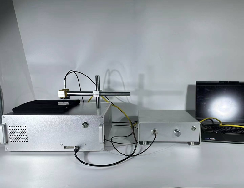
Industrial Two-Dimensional Film Thickness Measurement System
Fully automatic semiconductor film-thickness measurement system using visible light. White-light interference generally follows d=(wave2-wave1)/deltaWave*K, where wave denotes wavelength, deltaWave the two-peak wavelength difference and K refractive coefficient. It normally measures1um-100um films: Around200nm UV for 1um films, 500-600nm visible for 10-50um films, and 800nm infrared for films around80um. Above100um, calipers are recommended. Transparent films use transmission; opaque films such as semiconductor photoresist or aluminum lens coatings use reflection. XY motors enable automatic planar mapping with 150mm*150mm travel and customizable maximum1000mm*1000mm. An SPM3 UV-visible-near-IR hyperspectral thickness map shows thin regions blue and thick regions red. Douyin demonstration: https://www.douyin.com/user/self?modal_id=7363167072077057280 ; Bilibili: https://www.bilibili.com/video/BV1sH4y1V7CD/ . Integrated visible spectroscopy, a broad-spectrum long-life tungsten-halogen or xenon source, and a reflection probe support thin-film, semiconductor-coating and eyeglass-coating thickness measurements.
 Save to Favorites
Overview
Applications
Datasheet
Please provide your email to download the datasheet.
Invalid email format. Please try again.
Supplier Information
Related Products
-
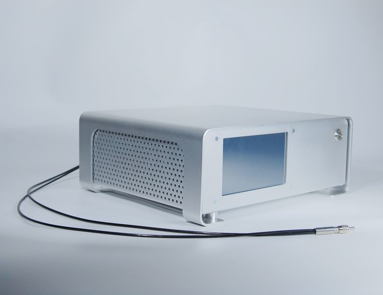 Optical System for Plastic Film Thickness Measurement UVS3-180-500
Optical Metrology
Jnewtech
Wavelength Range: 180-500nm Grating: 1200line/mm Resolution (FWHM) [MIN FWHM]: 0.2nm (MIN FWHM)
Plastic-film thickness optical system: UV xenon lamp, UV spectrometer and probe. White-light interference uses d = (wave2 - wave1)/deltaWave * K, where wave is wavelength, deltaWave the two-peak separation and K the refractive coefficient. Typical range is 0.5um -100um: approximately 200nm UV for 0.5um films, 500-600nm visible for 10-50um, and 800nm IR for around 80um. Above 100um, vernier calipers are recommended. Transparent films use transmission; opaque films, such as semiconductor etch endpoints, use reflection. A CMOS UV spectrometer and xenon source provide a cost-effective solution, with a JPN detector and USA/Germany hardware. 1. Integrated CMOS/xenon UV system simplifies measurement. 2. A high-performance flashing xenon lamp gives stable UV measurements. 3. Low-cost integration reduces complexity and provides a complete solution.
-
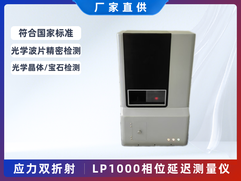 LP1000 Phase Retardation Measurement Instrument
Optical Metrology
Leice
Standard Light Source Wavelength: 633nm(632.8nm) Phase Retardation Measurement Interval: 0°~180° Measurement Repeatability: 0.2°
The LP1000 phase-retardation meter has received a second-class national invention award, and the company participated in drafting the national standard. Traceability, high precision, temperature compensation and multiwavelength conversion support stress and phase testing of waveplates, crystals and other optics. The core P1000 technology received the second-class National Technological Invention Award. We helped draft GB/T 26827-2011, Calibration Method for Waveplate Phase Retardation Measurement Devices. LP1000 is Leice's main traceable birefringence measurement model, intended for precision calibration of internal stress and phase retardation in optical elements. It tests transmissive materials such as waveplates, optical glass, display panels and crystals. A precision translation stage and temperature-compensation module are included, with customized nonstandard scanning solutions available.
-
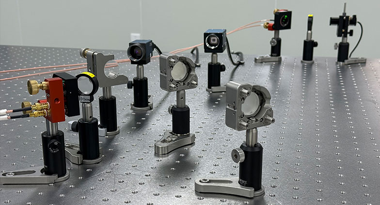 Beam-Pointing Stabilization System
Optical Metrology
Lumi-universe
Correction Capability [Single mirror, X,Y directions; correction range increases with multiple mirrors.]: Single mirror X,Y directions ± 0.4 mrad (correction range increases with multiple mirrors). Minimum Stride: ≤0.1μrad Direction LockingAccuracy [(@RMSE, Focal Point)]: ≤1urad (@RMSE, Focal Point)
In precision optics, thermal drift and stress relaxation can cause low-frequency beam disturbances and sustained spot drift. A highly sensitive camera detects disturbances in real time, while intelligent control dynamically steers an electrically controlled mirror to maintain a preset direction. Unlike other pointing-lock systems, camera detection with small pixels improves locking accuracy. During locking, users can observe spot shape and monitor beam power and its changes in real time.
-
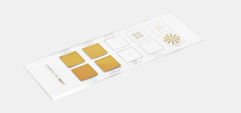 GMP-F Glass Mask Target
Optical Metrology
Oeabt
Specifications [±0.25]: 75*25*1.0mm(±0.25) Material: Quartz SiO₂, Chromium Coating Weight: 4.9g
Placing different masks, slits and apertures in the optical path at the Fourier plane before the beamsplitter allows pattern changes to be observed on the viewing screen.
-
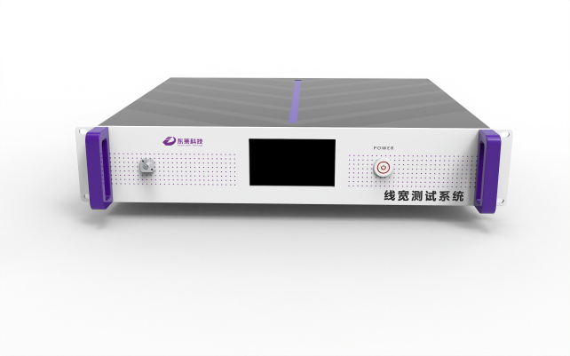 Laser Linewidth Test System
Optical Metrology
Dlphoton
Donglai Technology's laser linewidth test system uses delayed self-heterodyne interferometry, with an AOM as the interferometer's frequency shifter. The system includes a high-gain optical receiver/photodetector, a low-noise RF amplifier (LNA) and a high-resolution optical spectrum analyzer for measurement. High sensitivity permits measurement and analysis of laser linewidths down to 2kHz.
Related Articles
In photonics and laser technology, devices that manipulate optical signals via the electro-optic effect form the backbone of precision optical systems. Electro-optic phase modulators and electro-optic deflectors are two prominent examples of this device category. As a critical hardware solution for high-speed, high-accuracy laser beam direction control, electro-optic deflectors are widely deployed across industrial and research settings. Below is a detailed overview of their core structure, key performance drivers, and primary use cases.
As a top‑tier supplier of tunable laser chips, Shandong Zhongxin Optoelectronics Technology Company has newly launched the world’s first budget‑friendly fiber‑Bragg‑grating (FBG) demodulator and scanning module.
A laser bar is an array semiconductor laser chip integrated with dozens of emitters, which realizes hundred-watt quasi-continuous output on a single chip. With regular emitter arrangement and controllable fill factor, integrated thermal design and superior wall-plug efficiency compared to single chips, it acts as the core light source for high-power pumping, medical lasers and precision processing.
BEIJING JIEPU TREND supplies YAG+Er:YAG+YAG bonded composite slab laser crystals for high‑power solid‑state laser systems. The monolithic slab consists of two undoped YAG end‑cap layers and a central Er‑doped YAG gain segment. The overall dimension is 9 mm×9 mm×9 mm.
Loading...
Name
Phone
Organization
Use Case

Database Platform