


Specifications
| Parameter | Value |
|---|---|
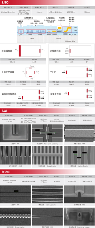
| LNOI Standard Wafer Size | 4 inches / 2 cm×2 cm |
| LNOI Feature Size | ≥150 nm; typical 1.4 μm |
| LNOI Typical Etch Depth | 250/300 nm |
| LNOI Center Wavelength | 1550 nm |
| SOI Standard Wafer Size | 15×15 mm, 20×20 mm, 4 inches |
| SOI Feature Size | ≥50 nm; typical 450/500/550 nm |
| SOI Typical Etch Depth | 220/340 nm |
| SOI Transmission Loss at 1550 nm | Expected ~2 dB/cm |
| Silicon Nitride Feature Size | Typical 1 μm |
| Silicon Nitride Typical Etch Depth | 300/800 nm |
| Silicon Nitride Transmission Loss at 1550 nm | Expected ~0.1 dB/cm |
Datasheet
Please provide your email to download the datasheet.
Invalid email format. Please try again.
Supplier Information
Related Products
-
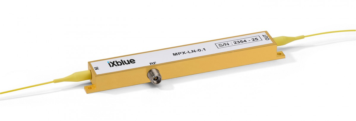 MPX-LN-0.1 optical phase modulator
EOM
Shconnet
MPX-LN-0.1 optical phase modulator
EOM
Shconnet
Electro-optic Bandwidth S_21 @ -3dB: 0.1GHz Half-Wave Voltage, RF Electrode @50kHz: 3V Input Impedance, RF Connector: 10000Ω
iXBlue's LiNbO3 optical phase modulators include the MPZ-LN series and the MPX-LN series, currently the most comprehensive electro-optic phase modulator product series on the market. The iXBlue MPZ-LN series LiNbO3 optical phase modulators combine low drive voltage and high modulation bandwidth, from 10GHz to over 20GHz.
-
 MPX2000-LN-0.1 optical phase modulator
EOM
Shconnet
MPX2000-LN-0.1 optical phase modulator
EOM
Shconnet
Wavelength Range: 1900nm Insertion Loss: 3dB Electro-Optical Bandwidth: 100MHz
iXBlue's MPX2000-LN-0.1 is an optical phase modulator specially designed for the 2.0um band, suitable for low-frequency applications (DC-150MHz). The MPX2000-LN-0.1 adopts a high-impedance modulation input interface, is easy to use, and has optimized low-frequency performance. The MPX2000-LN-0.1 uses a unique waveguide for the 2.0um band, with polarization-maintaining fiber input and output for the 2.0um band.
-
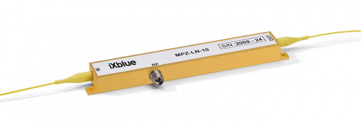 MPZ-LN-10 optical phase modulator
EOM
Shconnet
MPZ-LN-10 optical phase modulator
EOM
Shconnet
Electro-optic Bandwidth S_21 @ -3dB: 10GHz Half-Wave Voltage, RF Electrode @50kHz: 5.0V Half-Wave Voltage, RF Electrode @10GHz: 7.0V
iXBlue-Photonics' LiNbO3 optical phase modulators include the MPZ-LN series and the MPX-LN series, currently the most comprehensive electro-optic phase modulator product series on the market. The iXBlue-Photonics MPZ-LN series LiNbO3 optical phase modulators combine low drive voltage and high modulation bandwidth, from 10GHz to over 20GHz.
-
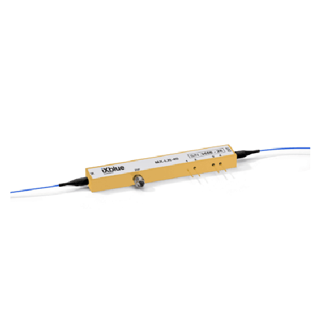 ixblue-Photline PV
EOM
Ovlink
ixblue-Photline PV
EOM
Ovlink
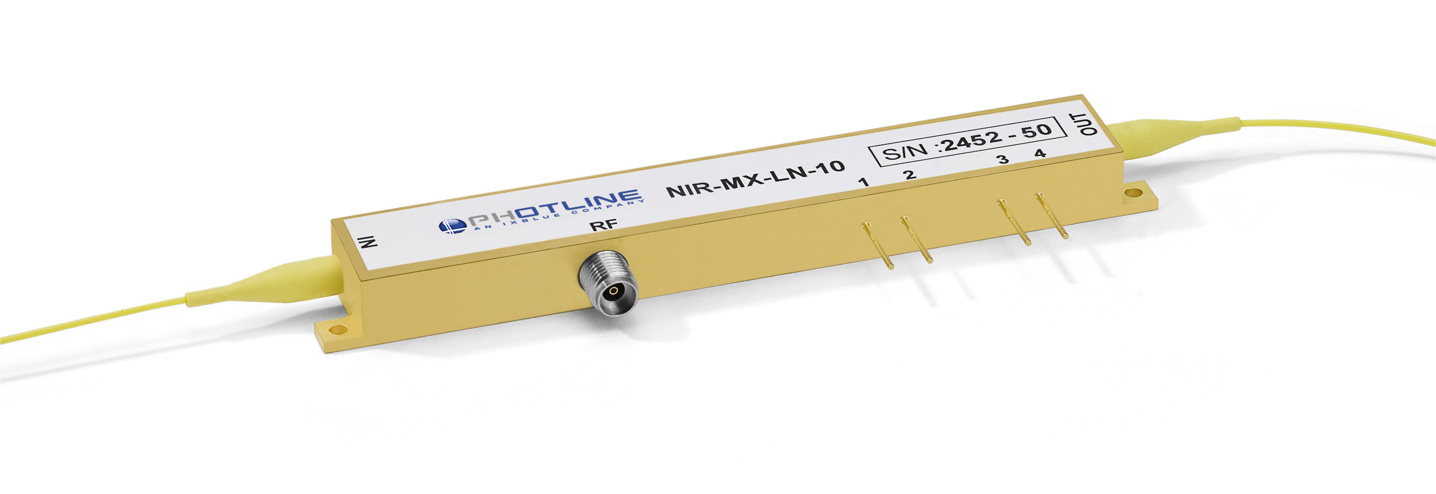
Photline, France, has the following options: lithium acrylic PVs; intensity moders; work wavelengths; 780-2200 nm optional (band option; 800 nm; 1000 nm; 1310nm; 550nm; 2000nm); electric bandwidth; DC-40GHz option; modem type optional; simulation strength moders; digital strength moders; high light relative strength moders; double output strength moders; double-frequency drive strength moders; IQ moders. Photline, France, is a lithium auracid PV moder; phase moder profile; working wavelength; 780-2200 nm optional (band option; 880 nm; 1,000 nm; 1550 nm; 2000nm); electric broadband; DC-40GHz option; mode type optional; X-Cut phase modem Z-Cut phase modem. Photline, France; Lithium Acrylic Optical Modems; Radio frequency driver profile; 10-40 GHz/Gb/s driver optional; simulation, digital driver optional; high pressure, low pressure driver optional; NRZ; RZ driver optional Select
Related Articles
As a professional manufacturer of precision optical thin-film components, sycco-optics (Shandong Yanggu Hengjing Optoelectronics) launches high-performance 850nm narrow band pass filters for near-infrared precision detection, intelligent sensing and optical imaging systems. Adopting advanced vacuum coating technology, the filter realizes high transmittance in the target band and deep blocking in interference bands. It effectively eliminates stray light and spectral noise, serving as a core optical component for machine vision, biochemical detection and photoelectric sensing equipment.
Wuhan Optics Valley Quantum Technology Co., Ltd. is a leading domestic developer of high‑speed semiconductor optical chips and photodetector components. Our product portfolio covers InGaAs avalanche photodiode bare dies and PIN photodetector chips designed for fiber‑optic communication
A microlens array (MLA) is a high-precision optical component composed of hundreds or thousands of tiny, uniformly arranged micro lenses on a single flat substrate. Unlike traditional single lenses that focus one light beam, a microlens array can split, homogenize, and reshape light on a micro scale. It is widely paired with VCSELs, lasers, and image sensors, becoming a core part of modern miniature optical systems.
Shandong Huaguang Optoelectronics Co., Ltd. (HAUCORE) is a leading high-tech manufacturer of compound semiconductor optoelectronic devices, founded in 1999 and headquartered in Jinan, China, with two R&D and production bases in Jinan and Weifang.
Loading...
Name
Phone
Organization
Use Case

Database Platform