
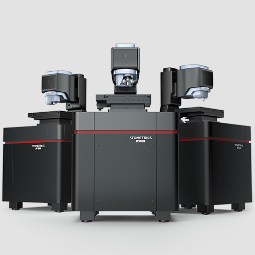
White Light Interferometer AM-8000 Series
While achieving high-precision measurement, the AM-8000 series also offers more efficient intelligent control: one-key automatic workpiece finding, focusing and leveling, with an XY-axis measurement range up to 300×300mm, meeting Mapping multi-point measurement, aspheric K-value measurement and other needs.; Compared with the AM-7000 series, the AM-8000 series platform has a 3x larger travel, 2.5x higher load capacity, 50% better positioning accuracy and 30% faster moving/stitching speed, supports more interferometric objectives and covers a wider range of application scenarios. Widely used in semiconductors, precision optics, 3C, new energy and other fields, providing efficient solutions for micro-nano structure measurement and roughness inspection.
 Save to Favorites
Overview
Specifications
| Parameter | Value |
|---|---|
| Accuracy | 0.03nm |
| XY Axis Measurement Range | Up to 300×300 mm |
| Stage Travel | 3 times improvement over the AM-7000 series |
| Load Capacity | 2.5 times improvement over the AM-7000 series |
| Positioning Accuracy | 50% improvement over the AM-7000 series |
| Travel Stitching Speed | 30% improvement over the AM-7000 series |
Applications
Datasheet
Please provide your email to download the datasheet.
Invalid email format. Please try again.
Supplier Information
Related Products
-
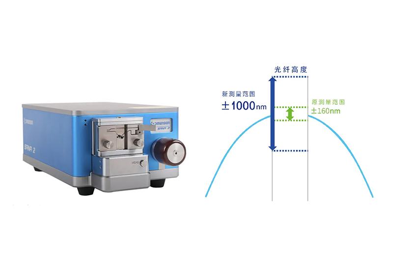 SANA2 fiber instrument
Interferometers
Dimension-tech
SANA2 fiber instrument
Interferometers
Dimension-tech
Power Supply Voltage: DC 24V
SANA 2 is a new manual focus autointerfer for the development of a new dimension technology;
-
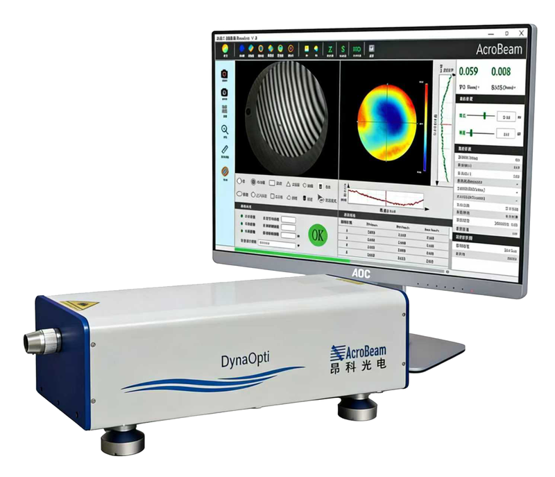 Dyna-Opti instrument
Interferometers
Acrobeam
Dyna-Opti instrument
Interferometers
Acrobeam
Instrument Aperture: 9mm, optional amplifier cal. 50-800mm Light: Importing ammonia lasers, 1 = 632.8 mm Camera: 2Kx2K pixel
Dyna-Opti series dynamic interferometer;
-
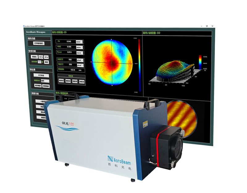 Digital Laser Interferometer
Interferometers
Acrobeam
Digital Laser Interferometer
Interferometers
Acrobeam
Interferometer Type: Fiso interferometer Measurement calibration: 60 mm, 4 inches (101.6 mm), 150 mm (other custom) Light: He-Ne laser (in = 632.8 nm)
Wavapex (the luminium series) digital laser interferometer;
-
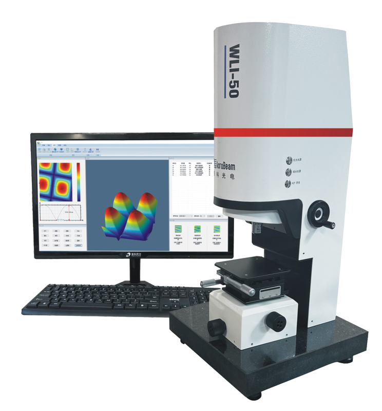 white-light series
Interferometers
Acrobeam
white-light series
Interferometers
Acrobeam
Objective Lens: Infinite interference mirrors 2.5X, 5X, 10X, 20X, 50X (other customable); Infinite intervention lenses 10X (20X optional) Lateral Resolution: 0.4um ~10.2um, related to selected mirrors
The WLI series of white light interferometers are based on white light interferometry;
-
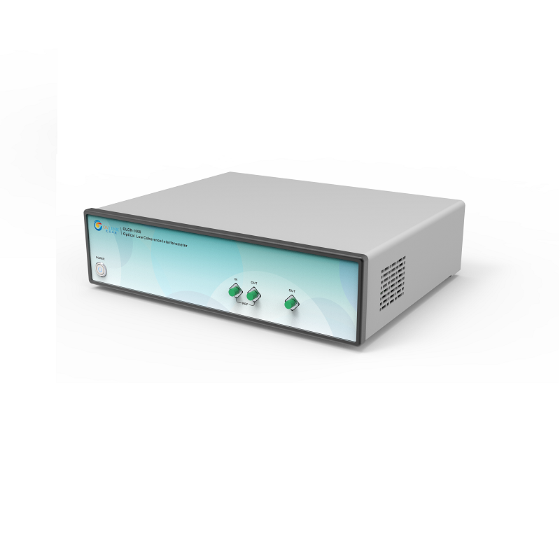 Low-linked light interferometer OCR
Interferometers
Ovlink
Low-linked light interferometer OCR
Interferometers
Ovlink
Work wavelength: 1310 & 1550nm Measuring length: 50; condition: other measurements can be determined Production Time-consuming single measurement: ^15s
Low-continental light interferometer OLCR-1000 is a distributed fibre-optic reruption detection system based on white light interferometry; detectability recognition that can be used for fibre-optic microfracking, optical devices, photochip reflectors; and have the advantage of being low-cost, high-precision measurement and short time-consuming relative to optical-frequency reflectors. Second-scale measurements; quick-output measurements; micro-level positioning; accurate identification of various reflex events; high-precision backsliding measurements; accurate output of reflection events backsliding; sub-miscale measurements range; greater measurement length customizable
Related Articles
Precise spectral screening is essential for high-precision medical detection, spectroscopic analysis and intelligent imaging systems. Tailored for visible and near-infrared spectral separation, the SP900 shortpass optical filter delivers high-efficiency light transmission and deep infrared blocking performance. It effectively eliminates stray light interference, improves signal-to-noise ratio (SNR), and serves as a core optical component for biomedical instruments, scientific analysis equipment and machine vision systems.
As a professional ultraviolet‑laser solution provider, Precilasers has launched its 266 nm narrow‑linewidth industrial laser, delivering reliable single‑frequency output for high‑precision interference lithography, semiconductor inspection and precision metrology applications.
Founded in November 2017, TIANJIN H‑CHIP TECHNOLOGY GROUP CORPORATION is a professional manufacturing‑service provider dedicated to micro‑nano optoelectronic chips. It holds multiple prestigious qualifications, including National High‑Tech Enterprise, one of Tianjin’s first Gazelle‑certified Enterprises, Specialized‑Refined‑Differentiated‑Innovative SME, and Leading Enterprise for Strategic Emerging Industries.
Recently, the key laboratory of Functional Crystal Materials of Tianjin University has published a cutting-edge research paper titled Enhanced Second-Harmonic Generation in Quadratically Nonlinear Weyl Semimetal NbAs for Broadband Photodetection Applications on Advanced Science, a top-tier international academic journal.
Loading...
Name
Phone
Organization
Use Case

Database Platform