
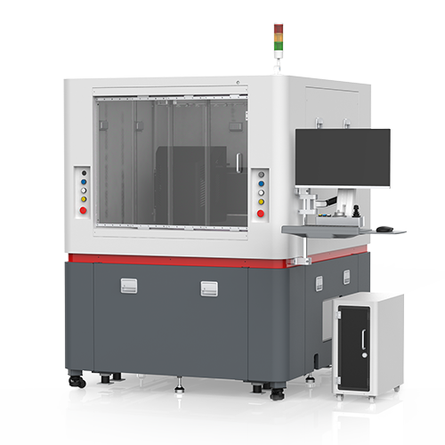
Package Substrate 3D Automatic Inspection Equipment Elite Pro Series
Ultra-fast scanning speed: vertical scanning speed 5 times that of conventional models; Fully automatic measurement: extremely simple operation, easy online programming settings, automatic measurement; Offline analysis: original data can be retrieved for secondary specific analysis; Offline editing: offline editing through ODB++ programs (optional); Rich measurement functions.
 Save to Favorites
Overview
Specifications
| Parameter | Value |
|---|---|
| Vertical Scan Speed | 5 times that of traditional models |
Applications
Datasheet
Please provide your email to download the datasheet.
Invalid email format. Please try again.
Supplier Information
Related Products
-
 Covered for the job
Packages
Gan-semi
Covered for the job
Packages
Gan-semi
-
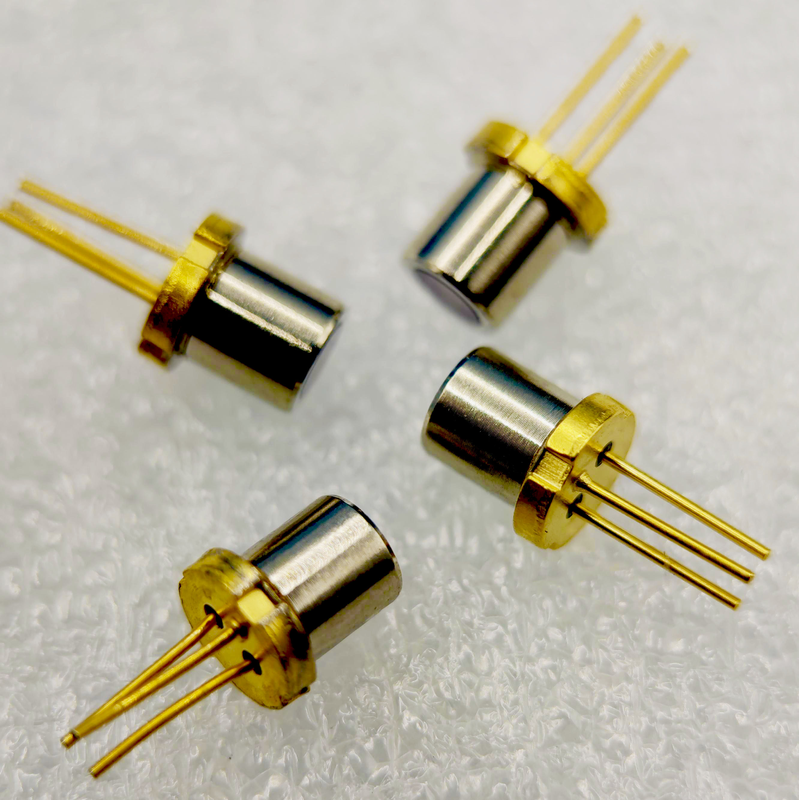 660 nm 120 mW TO56 for red light lasers
Packages
Iqpackage
660 nm 120 mW TO56 for red light lasers
Packages
Iqpackage
Seal Size: TO56 Materials: Deforestable alloy/copper Wavelength: 660nm
-
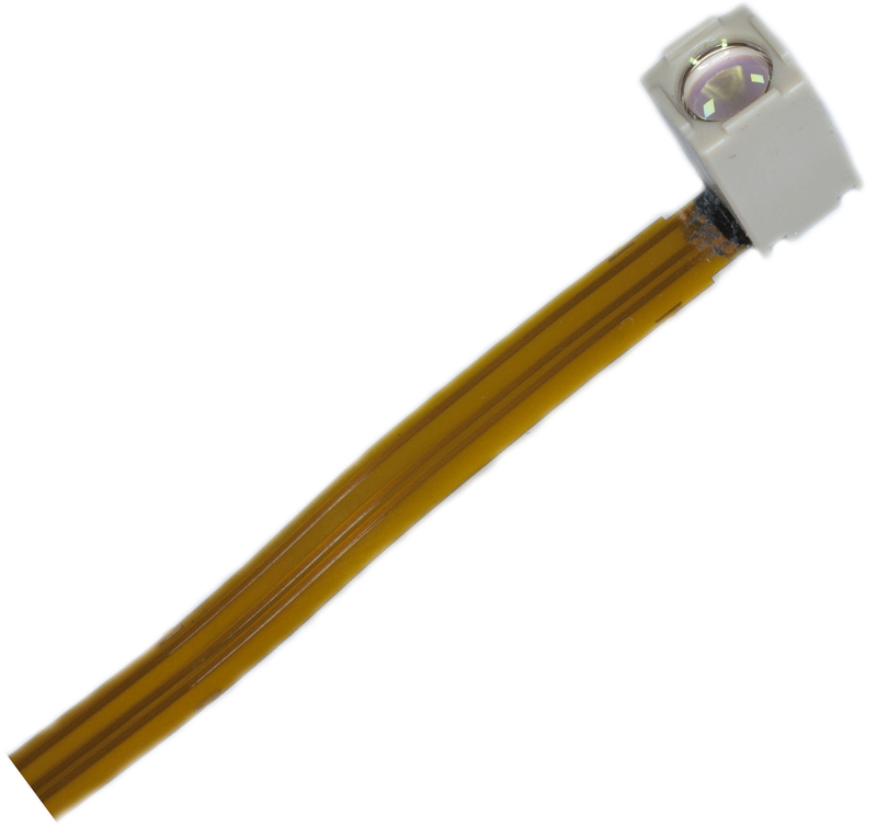 795 nm without magnetic encapsulation laser
Packages
Iqpackage
795 nm without magnetic encapsulation laser
Packages
Iqpackage
Wavelength: 795nm Light angle: 0.5 Light power: 1.4mW
-
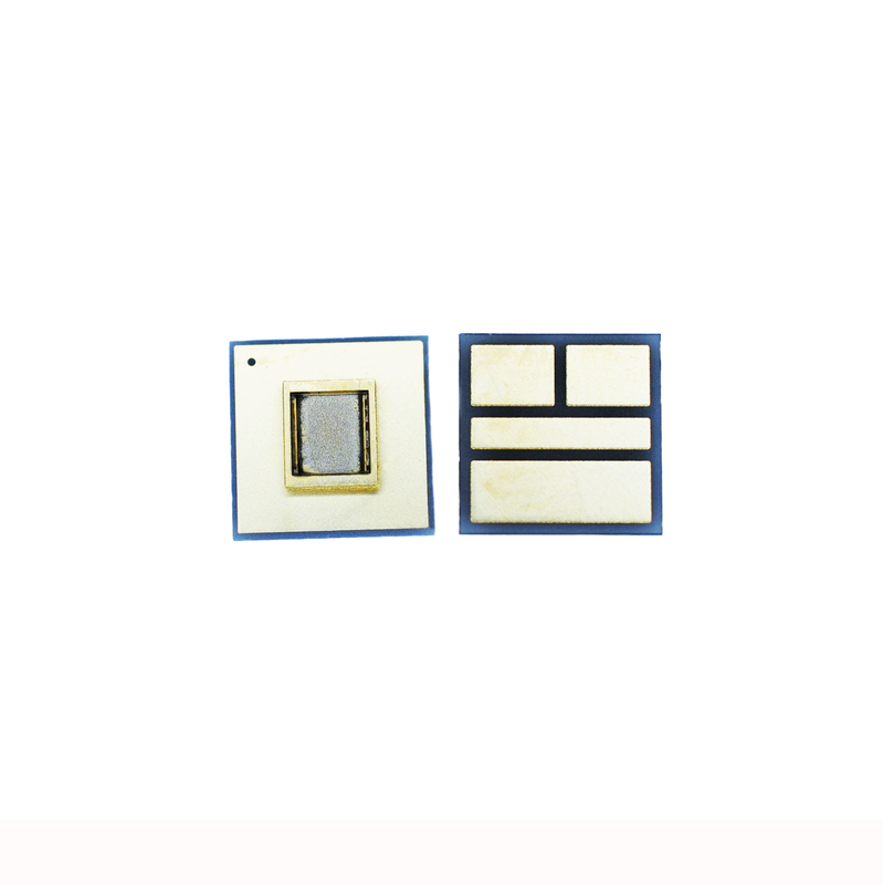 940 nm3JVCSEL7070 lasers
Packages
Iqpackage
940 nm3JVCSEL7070 lasers
Packages
Iqpackage
Seal Size: 7.0x7.0x1.72mm Materials: Ceramic Driver current: 3.5A
-
 Prefabricated tin
Packages
Gem-oe
Prefabricated tin
Packages
Gem-oe
Gold tin film welds: Au/Sn=70~80/30~20 Membrane thickness: 3 micro, 5 micro Weld temperature: 290~320℃
Related Articles
As a professional manufacturer of precision optical thin-film components, sycco-optics (Shandong Yanggu Hengjing Optoelectronics) launches high-performance 850nm narrow band pass filters for near-infrared precision detection, intelligent sensing and optical imaging systems. Adopting advanced vacuum coating technology, the filter realizes high transmittance in the target band and deep blocking in interference bands. It effectively eliminates stray light and spectral noise, serving as a core optical component for machine vision, biochemical detection and photoelectric sensing equipment.
Wuhan Optics Valley Quantum Technology Co., Ltd. is a leading domestic developer of high‑speed semiconductor optical chips and photodetector components. Our product portfolio covers InGaAs avalanche photodiode bare dies and PIN photodetector chips designed for fiber‑optic communication
A microlens array (MLA) is a high-precision optical component composed of hundreds or thousands of tiny, uniformly arranged micro lenses on a single flat substrate. Unlike traditional single lenses that focus one light beam, a microlens array can split, homogenize, and reshape light on a micro scale. It is widely paired with VCSELs, lasers, and image sensors, becoming a core part of modern miniature optical systems.
Shandong Huaguang Optoelectronics Co., Ltd. (HAUCORE) is a leading high-tech manufacturer of compound semiconductor optoelectronic devices, founded in 1999 and headquartered in Jinan, China, with two R&D and production bases in Jinan and Weifang.
Loading...
Name
Phone
Organization
Use Case

Database Platform