
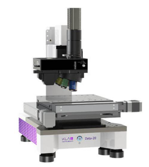
Zeta-20
The Zeta-20 optical profiler is a versatile and precise measurement tool designed for surface characterization and analysis. It offers advanced imaging capabilities and multi-mode operation for various applications.
 Save to Favorites
Overview
Specifications
| Parameter | Value |
|---|---|
| Measurement Range | 0.1nm to 1mm |
| Resolution | 0.1nm |
| Field of View | 50μm to 10mm |
| Objective Lenses | 5x, 10x, 20x, 50x |
| Light Source | White light LED |
| Stage Size | 200mm x 200mm |
| Data Output | 3D surface maps, 2D profiles |
| Software | Zeta software suite |
Applications
Key Features
Datasheet
Supplier Information
Related Products
-
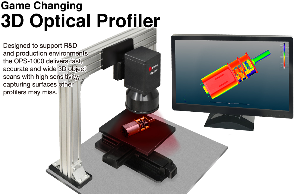 OPS-1000 3D Optical Profiler
Optical Surface Profiler
Santec
OPS-1000 3D Optical Profiler
Optical Surface Profiler
Santec
Scanning Range: Wide Sensitivity: High Scanning Speed: Fast
The OPS-1000 is designed to support R&D and production environments, delivering fast, accurate, and wide 3D object scans with high sensitivity, capturing surfaces other profilers may miss.
-
 Keyence Laser Displacement Sensor
Optical Surface Profiler
Keyence
Keyence Laser Displacement Sensor
Optical Surface Profiler
Keyence
Measuring Range: 20mm-200mm Resolution: 0.01mm Sampling Speed: 80kHz
The Keyence Laser Displacement Sensor is a high-precision measurement device designed for accurate distance and position detection in various industrial applications.
-
 Zeta-300
Optical Surface Profiler
Ybsemi-Solution
Zeta-300
Optical Surface Profiler
Ybsemi-Solution
Scanning Range: 280μm Sample Stage Size: 150×150mm, 200×200mm, 300×300mm Imaging Resolution: 5MP
Zeta-300 is a fast, non-contact 3D optical profiler designed for precise surface measurement and analysis.
-
 Tencor P-170 Stylus Profiler
Optical Surface Profiler
Ybsemi-Solution
Tencor P-170 Stylus Profiler
Optical Surface Profiler
Ybsemi-Solution
Scan Length: ≤200mm Vertical Range: ≤1mm Force Control Range: 0.03g-50g
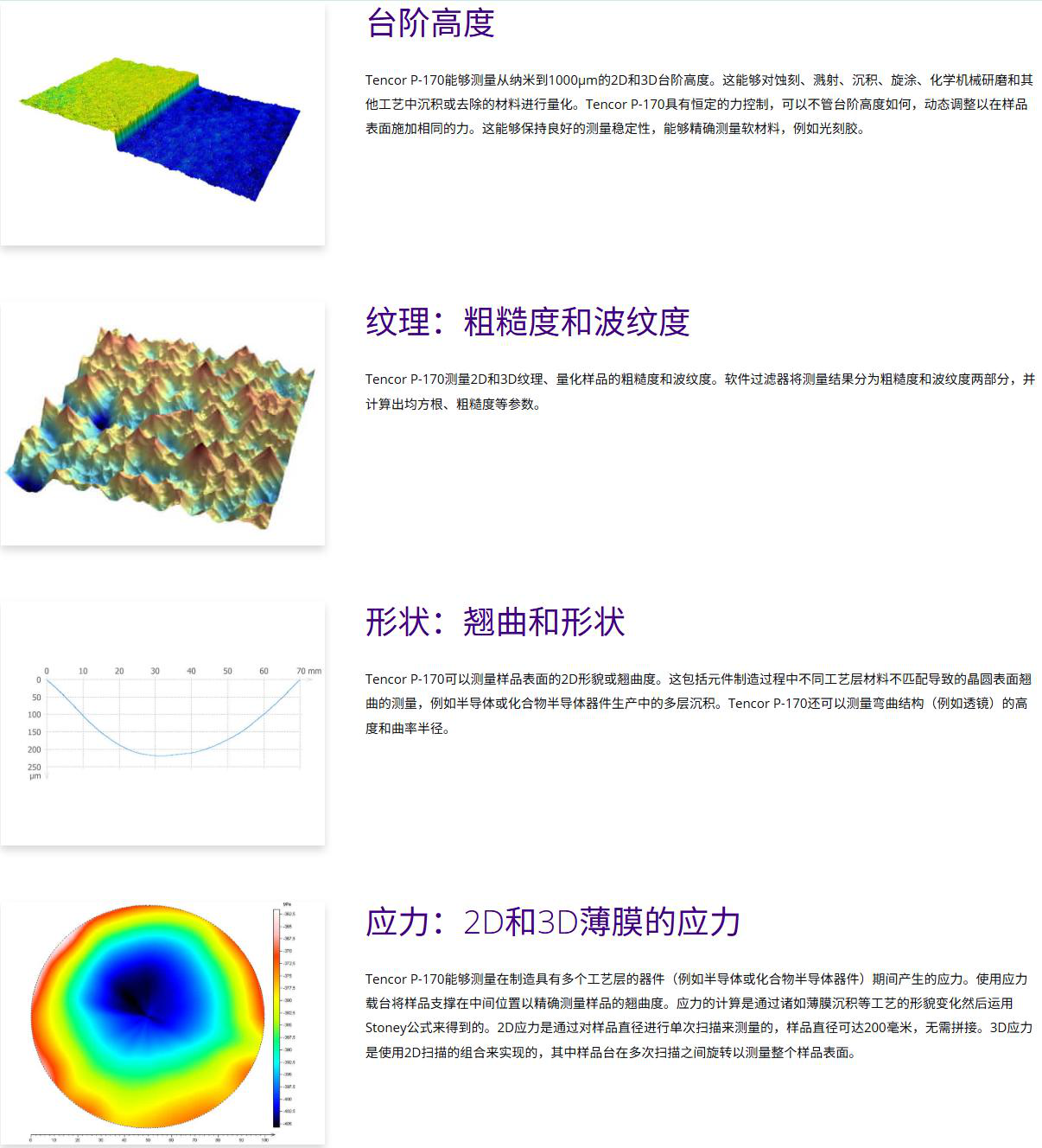
The Tencor P-170 Stylus Profiler is a cassette-to-cassette system designed for high-precision surface measurement. It offers advanced capabilities for 2D and 3D scanning, step height measurement, roughness analysis, and thin film stress evaluation, making it ideal for semiconductor, LED, MEMS, and data storage applications.
-
 Zeta-388 Optical Profiler
Optical Surface Profiler
Ybsemi-Solution
Zeta-388 Optical Profiler
Optical Surface Profiler
Ybsemi-Solution
Optical Resolution: 5MP Sample Size Range: 45×35μm to 9.5×7.5mm Film Thickness Range: 30nm to 100μm
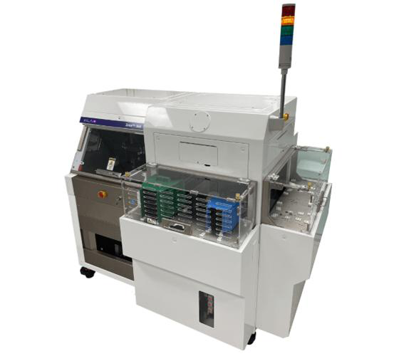
The Zeta-388 optical profiler is a non-contact, 3D surface topography measurement system designed for automated defect inspection and precise measurements of step heights, roughness, and film thickness. It features ZDot™ technology and multi-mode optics for high-resolution imaging.
Related Articles
Shanghai Connet Laser Technology Co., Ltd. focuses on technological innovation, delivering cutting-edge photonic products & solutions for industrial lasers, LiDAR, fiber optic sensing, coherent telecom, cold atom physics and precision spectroscopy research & mass manufacturing.
A solid-state laser is one of the most common and reliable laser types used in modern industry, medical equipment, and scientific research. Unlike gas or fiber lasers, it uses solid materials as its gain medium to generate stable, high-brightness laser beams. Thanks to its high precision, long lifespan, and compact structure, solid-state lasers have become a mainstream solution for high-precision laser processing and optical systems.
Looking for a market-verified 808nm pump laser diode? This guide introduces HAUCORE DM-8E5A-8OD (HGLD-808-COS-D-5W), its core advantages, key specs and mainstream industrial, medical & research applications.
Founded in 2003, BWT Beijing Optoelectronics adheres to the mission "Let Dreams Fly With Light" and vision of becoming a Global Leader in Laser Solutions, guided by the core value "Innovate to Achieve Extraordinary".
Loading...
Name
Phone
Organization
Use Case

Database Platform