
X-Ray Detector XRD-C
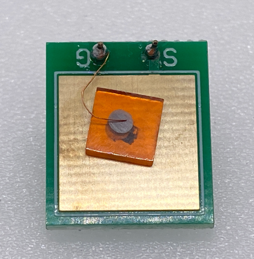
These independently developed X-ray detectors combine internally prepared high-quality radiation-detection crystals, precision electrodes and low-noise electronics. Semiconductor direct conversion turns X-ray ionization into electrical pulses, balancing efficiency, energy resolution and flexible integration in a compact volume. CdTe and perovskite versions support single-element detection, spectroscopy, linear/area imaging and special structures. Crystal size/thickness, electrodes, package window, front-end circuitry and interfaces are customizable. X-rays deposit energy through photoelectric absorption and other processes, generating electron–hole pairs. An applied field drifts carriers to opposing electrodes, forming energy-related charge pulses. Low-noise preamplification, shaping and digitization yield count rate, spectra or 2D images. Direct conversion eliminates scintillator/optical-conversion stages for compactness and preserved energy information.
 Save to Favorites
Overview
Specifications
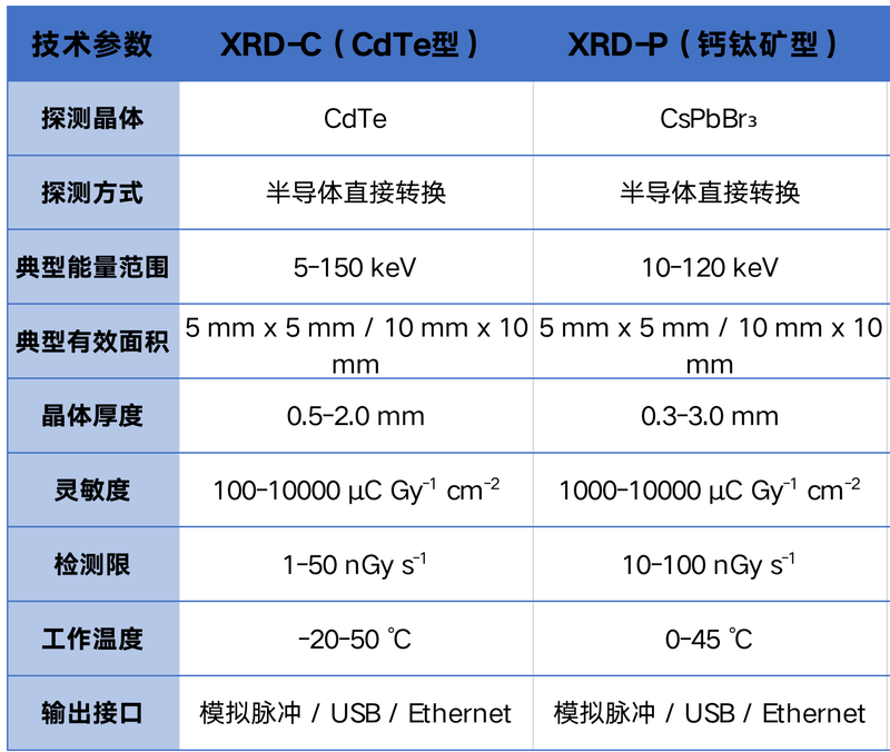
| Parameter | Value |
|---|---|
| Detection Crystal | CdTe |
| Detection Method | Semiconductor Direct Conversion |
| Typical Energy Range | 5-150keV |
| Typical Effective Area | 5mm x 5mm / 10mm x 10mm |
| Crystal Thickness | 0.5-2.0mm |
| Sensitivity | 100-10000μC Gy⁻¹ cm⁻² |
| Detection Limit | 1-50nGy s⁻¹ |
| Operating Temperature | -20-50°C |
| Output Interface | Analog Pulse / USB / Ethernet |
Applications
Key Features
Datasheet
Please provide your email to download the datasheet.
Invalid email format. Please try again.
Supplier Information
Related Products
-
 40G High-Speed Indium Gallium Arsenide (InGaAs) Photodetector HSPD4040
Optical Detectors
Fiberwdm
Storage Temperature Range TSTG [Typical Values and Absolute Maximum Ratings]: typical:-45~+85; Rated: -55~+85 Operating Case-Temperature Range TC [Typical Values and Absolute Maximum Ratings]: typical:25; Rated: -40~+85 Bias Voltage VR [Typical Values and Absolute Maximum Ratings]: typical:5; Rated: 5~6
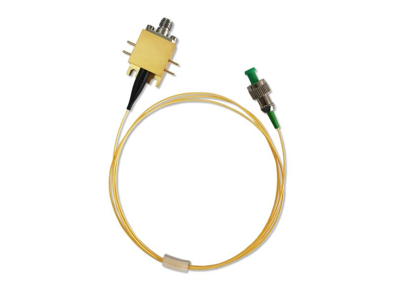
HSPD4040 is a high-speed detector module for digital/analog applications. An InGaAs PIN photodiode responds over1250–1650nm with matching electronics. Maximum bandwidth is40GHz, supply+5V, input standard single-mode9/125μm fiber, and RF output a2.92mm connector matched to50ohms. A sealed housing weighs under20g. The description states ROHS2.0 compliance with restrictions on hazardous substances in electrical/electronic equipment. After nearly two years of R&D,广州瑞东 developed two fully domestic high-speed PD products described as exceeding18GHz and40GHz bandwidth. The18GHz version has rise time<20ps and the40GHz PD<8.5ps. Responsivity is described as matching or exceeding comparable Finisar/Thorlabs imports,with well-controlled tail ringing. Without a TIA,the detectors provide very low noise for high-speed communications and femtosecond-laser testing at high cost effectiveness. The company's independently developed linear supply meets research needs for these detectors.
-
 Biased Detector Series PD1500/PD2100
Optical Detectors
Fiberwdm
Wavelength Range: 900nm-1700nm 3dB Cutoff Bandwidth: 5GHz Saturation Optical Power: 5mW
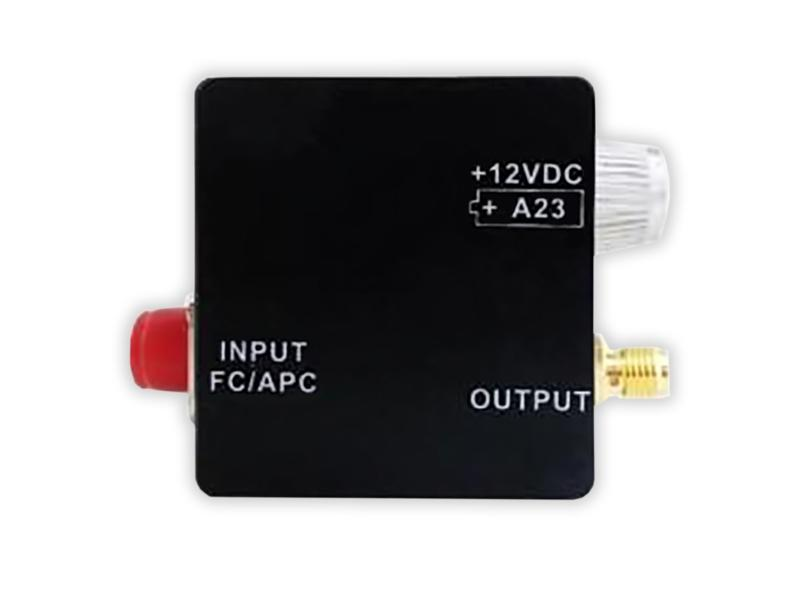
This detector series is a direct replacement for Thorlabs battery-powered products and is described as matching or exceeding equivalent Thorlabs products in all performance aspects. In addition to standard specifications, customization can adjust parameters such as supply voltage and bandwidth to customer requirements. Designed specifically for laser measurement systems, the series has an internal battery and no gain amplification, offering a cost-effective detector for high-power laser laboratories.
-
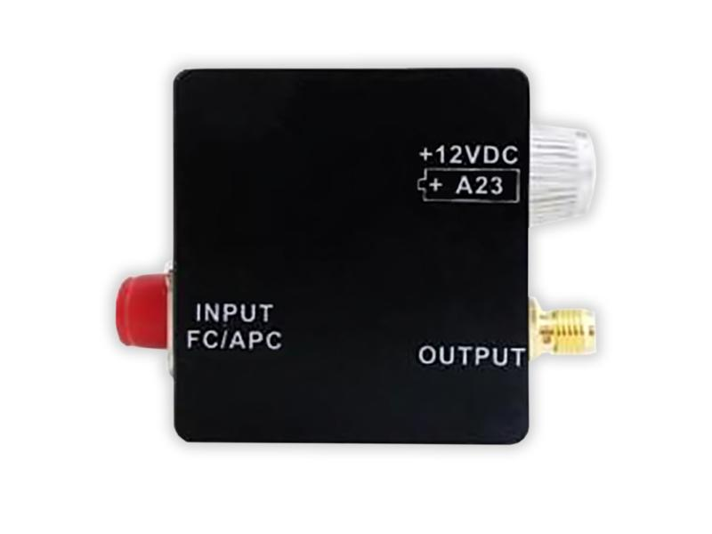 Biased Detector Series PD1500/PD2100
Optical Detectors
Fiberwdm
Wavelength Range: 320nm-1000nm 3dB Cutoff Bandwidth: 1GHz Saturation Optical Power: 5mW
This detector series is a direct replacement for Thorlabs battery-powered products and is described as matching or exceeding equivalent Thorlabs products in all performance aspects. In addition to standard specifications, customization can adjust parameters such as supply voltage and bandwidth to customer requirements. Designed specifically for laser measurement systems, the series has an internal battery and no gain amplification, offering a cost-effective detector for high-power laser laboratories.
-
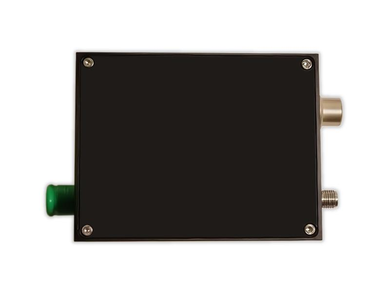 High-Speed Detector HSPD4018
Optical Detectors
Fiberwdm
Wavelength Range: 1000nm - 1700nm 3dB Cutoff Bandwidth: 18GHz Conversion Gain: 35V/W
After nearly two years of R&D,广州瑞东 developed two fully domestic high-speed PD products described as exceeding18GHz and40GHz bandwidth. The18GHz version has rise time<20ps and the40GHz PD<8.5ps. Responsivity is described as matching or exceeding comparable Finisar/Thorlabs imports,with well-controlled tail ringing. Without a TIA,the detectors provide very low noise for high-speed communications and femtosecond-laser testing at high cost effectiveness. The company's independently developed linear supply meets research needs for these detectors.
-
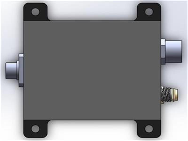 PDA1000-2 Dual-Channel 10KHz Single-Element Detector
Optical Detectors
Fiberwdm
Wavelength Range [Model PDA1000-2 in the Technical Table]: 900-1700nm dB Bandwidth [Model PDA1000-2 in the Technical Table]: 10kHz Conversion Gain [Technical Table Model PDA1000-2; High-Impedance Output Load; Gain Halved from Nominal with 50Ω Load]: 2.5×10⁴V/A
This detector series operates much like single-element detectors from Thorlabs and Newport and has identical power interfaces. It can directly replace equivalent products when Monitor output is unnecessary and bandwidth matches, with performance described as matching or exceeding comparable Thorlabs/Newport detectors. Beyond standard versions, customization adjusts supply voltage, gain, bandwidth and other parameters to customer requirements.
Related Articles
Founded in 2019, Jilin JC Ultrafast Equipment Co., Ltd. is a high-tech enterprise incubated by the Ultrafast Optoelectronics Center of Jilin University. Our R&D team owns 15 years of profound experience in femtosecond laser micro-nano fabrication.
VCSEL, short for Vertical Cavity Surface Emitting Laser, is a widely used semiconductor laser component in modern optoelectronics. Unlike traditional edge-emitting lasers, VCSEL emits laser light vertically from its chip surface. Thanks to its low power consumption, stable beam quality, low cost, and easy integration, it has become the core light source for 3D sensing, wearable devices, and high-speed optical communication.
Driven by the rapid upgrading of intelligent vehicles, optoelectronic sensing technologies represented by laser sensing and infrared thermal imaging have become core pillars for high-level autonomous driving and smart cockpit iteration. Leveraging automotive-grade optoelectronic R&D advantages, Pilot Technology Group launches the VITAL intelligent vehicle solution. By integrating high-power VCSEL laser chips and vehicle infrared night-vision thermal imagers, the system comprehensively enhances vehicle environmental perception and realizes safer, smarter and more comfortable driving experiences.
The MSL‑T series water‑cooled continuous‑wave single‑longitudinal‑mode lasers from Changchun New Industries Optoelectronics (CNI) deliver key research wavelengths including 369 nm, 405 nm and 770 nm.
Loading...
Name
Phone
Organization
Use Case

Database Platform