
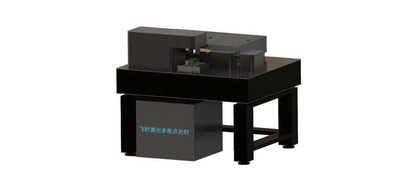
Femtosecond Laser Multifocus Holographic Lithography System
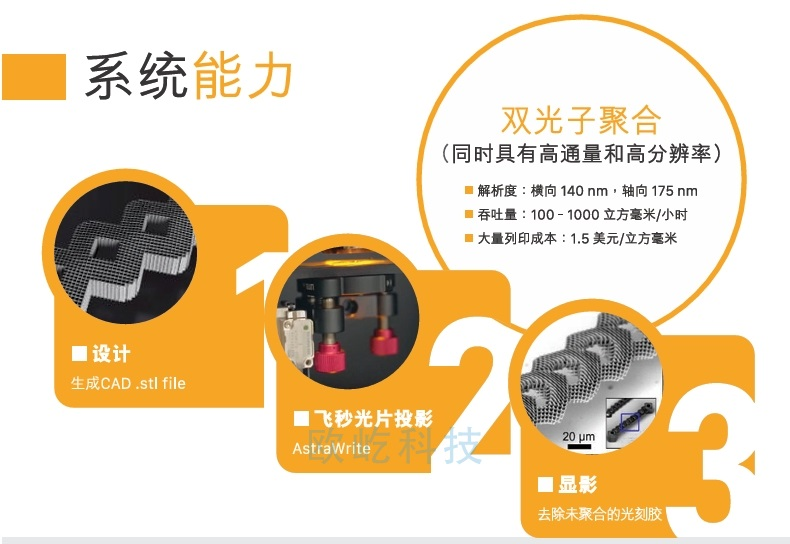
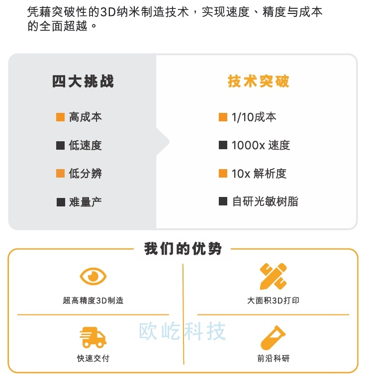
Femtosecond laser multifocus holographic lithography has gained international recognition and several successful U.S. applications… By substantially reducing micro-additive manufacturing costs, FP NanoPrinter enables 3D printing at 30nm resolution and industrial scale multimaterial 3D nanofabrication. This technology opens new possibilities for precision injection molding, optics, biomedicine, chips and metamaterials.
 Save to Favorites
Overview
Specifications
| Parameter | Value |
|---|---|
| relative humidity | < 50% (< 35% Recommended ) |
| Printing Technology | Projection Lithography |
| Minimum Feature Size (XY / Z) | 142 nm* / 175 nm* |
| Resolution (Diffraction Limit, XY / Z) | 285 nm* / 500 nm* |
| Layer Spacing | ≥0.05µm* |
| Printing Rate | 100 mm ³ /hr* |
| Parallel Writing Foci | ≥100 |
| Multifocus Control | Any Single Focus Point Editing and Control |
| Small Surface Roughness | ≤ 20 nm |
| Laser Safety | Class 4 |
| Software | Including |
| AstraWrite | Dedicated GUI |
| Data Input | Various Image Files (.bmp, .stl) |
| Weight (Without Optical Table) | 500 kg |
| Operating Temperature | 23 ± 1 ℃ |
| Room Illumination | ≥ 590 nm During Operation Illumination |
| Particles | Class 10000 |
| Power Supply | 220V, > 35 A |
| Vibration Class | Vibration Isolation and Damping Required ; No Vibration Sources in Room |
| Compressed Air Supply | 0.55 ±0.03MPa, flow 40 SLPM |
| Ambient Air Requirements | 20 cm Range No Noticeable Airflow Within |
| Altitude | High 2500 m |
Key Features
Datasheet
Please provide your email to download the datasheet.
Invalid email format. Please try again.
Supplier Information
Related Products
-
 Post-Evaporation Inspection System
Semiconductor Manufacturing Equipment
Lic-vision
-
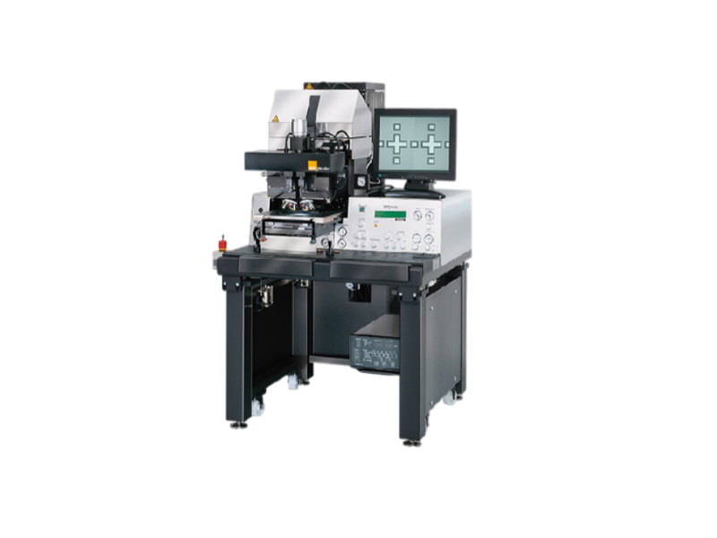 Lithography System
Semiconductor Manufacturing Equipment
Trusee
-
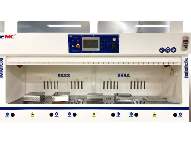 Resist Stripping System
Semiconductor Manufacturing Equipment
Trusee
-
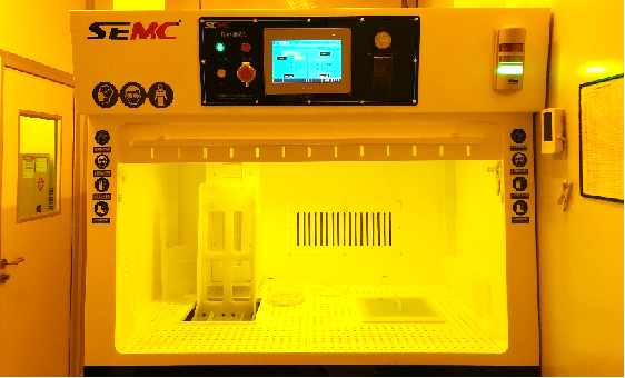 Developing System
Semiconductor Manufacturing Equipment
Trusee
-
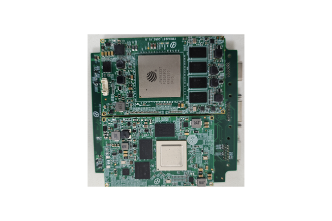 Image Recognition and Tracking Board
Semiconductor Manufacturing Equipment
Tera-aurora
Main Processor [FPGA]: Fudan Micro 7K325t Main Processor [ARM]: HiSilicon 3403 Storage [FPGA]: 32G EMMC, 64G SD Card
Image Recognition and Tracking Board
Related Articles
As a core precision optical component for wavelength screening, frequency locking and spectral demodulation, optical etalons are widely used in high-end scientific research and precision laser equipment.
Shanghai Connet Laser Technology Co., Ltd. focuses on technological innovation, delivering cutting-edge photonic products & solutions for industrial lasers, LiDAR, fiber optic sensing, coherent telecom, cold atom physics and precision spectroscopy research & mass manufacturing.
A solid-state laser is one of the most common and reliable laser types used in modern industry, medical equipment, and scientific research. Unlike gas or fiber lasers, it uses solid materials as its gain medium to generate stable, high-brightness laser beams. Thanks to its high precision, long lifespan, and compact structure, solid-state lasers have become a mainstream solution for high-precision laser processing and optical systems.
Driven by worldwide energy‑structure transformation, the lithium‑ion battery industry is expanding rapidly as green, high‑efficiency energy‑storage devices gain surging global market demand. With years‑long dedication to intelligent manufacturing, Han’s Laser Lithium‑battery Intelligent Equipment has accumulated solid R&D strength and rich practical experience. By integrating multiple cutting‑edge technologies, the company delivers high‑efficiency, eco‑friendly and sustainable lithium‑ion battery production lines, bringing revolutionary upgrades to the new‑energy battery sector.
Loading...
Name
Phone
Organization
Use Case

Database Platform