
Maskless DLP Projection Lithography System
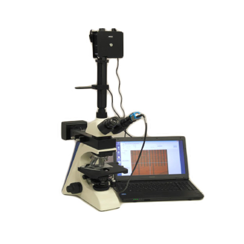
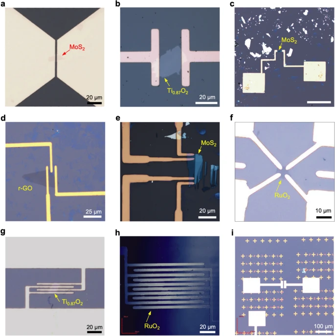
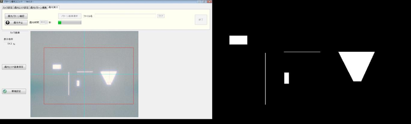
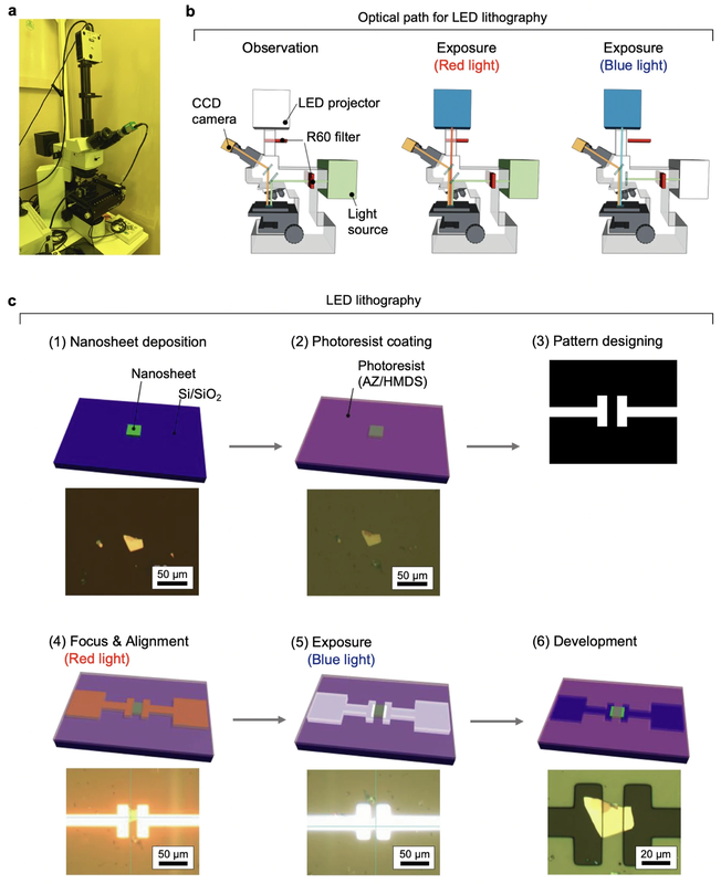
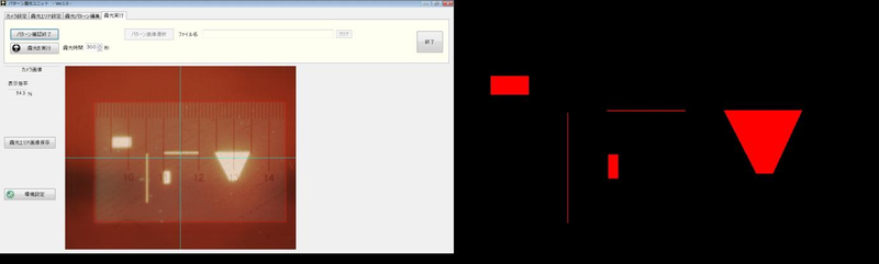
The UTA microscope LED exposure unit is a maskless pattern projection device for photolithography. A metallurgical microscope and LED DLP projector expose arbitrary patterns at micrometer resolution on resist coated substrates. Patterns can be freely created on a PC. Electrodes can be formed on single crystal flakes of various sizes and shapes under ordinary indoor conditions. The process is cheaper and simpler than electron beam lithography and eliminates expensive electrode pattern masks.
 Save to Favorites
Overview
Specifications
| Parameter | Value |
|---|---|
| min scale | 1 μm |
| Exposure Range | max:2.5mm×1.5mm; min:100μm×60μm |
Applications
Datasheet
Please provide your email to download the datasheet.
Invalid email format. Please try again.
Supplier Information
Related Products
-
 Post-Evaporation Inspection System
Semiconductor Manufacturing Equipment
Lic-vision
-
 Lithography System
Semiconductor Manufacturing Equipment
Trusee
-
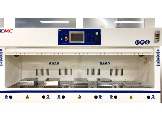 Resist Stripping System
Semiconductor Manufacturing Equipment
Trusee
-
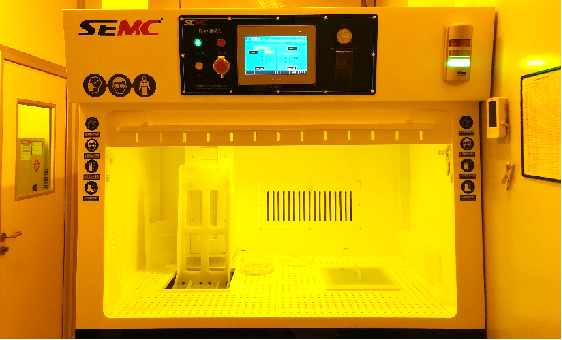 Developing System
Semiconductor Manufacturing Equipment
Trusee
-
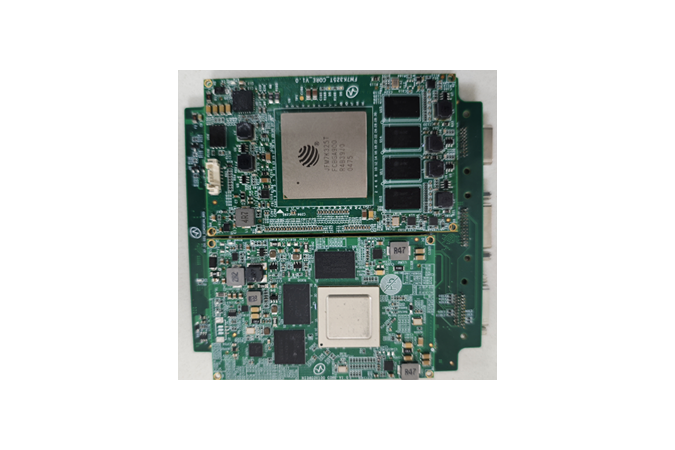 Image Recognition and Tracking Board
Semiconductor Manufacturing Equipment
Tera-aurora
Main Processor [FPGA]: Fudan Micro 7K325t Main Processor [ARM]: HiSilicon 3403 Storage [FPGA]: 32G EMMC, 64G SD Card
Image Recognition and Tracking Board
Related Articles
As a core precision optical component for wavelength screening, frequency locking and spectral demodulation, optical etalons are widely used in high-end scientific research and precision laser equipment.
Shanghai Connet Laser Technology Co., Ltd. focuses on technological innovation, delivering cutting-edge photonic products & solutions for industrial lasers, LiDAR, fiber optic sensing, coherent telecom, cold atom physics and precision spectroscopy research & mass manufacturing.
A solid-state laser is one of the most common and reliable laser types used in modern industry, medical equipment, and scientific research. Unlike gas or fiber lasers, it uses solid materials as its gain medium to generate stable, high-brightness laser beams. Thanks to its high precision, long lifespan, and compact structure, solid-state lasers have become a mainstream solution for high-precision laser processing and optical systems.
Driven by worldwide energy‑structure transformation, the lithium‑ion battery industry is expanding rapidly as green, high‑efficiency energy‑storage devices gain surging global market demand. With years‑long dedication to intelligent manufacturing, Han’s Laser Lithium‑battery Intelligent Equipment has accumulated solid R&D strength and rich practical experience. By integrating multiple cutting‑edge technologies, the company delivers high‑efficiency, eco‑friendly and sustainable lithium‑ion battery production lines, bringing revolutionary upgrades to the new‑energy battery sector.
Loading...
Name
Phone
Organization
Use Case

Database Platform