
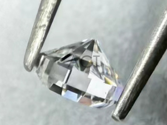
Diamond Anvil
High hardness, good thermal conductivity and chemical inertness make diamond an ideal opposed-anvil material for research in materials science, earth science and chemistry. We offer low-stress, flawless, low-fluorescence diamond anvils in Standard, Boehler and Diacell shapes, with custom dimensions and structures available.
 Save to Favorites
Overview
Specifications
| Parameter | Value |
|---|---|
| Diameter [Standard Type (standard design)] | 2.5-4mm |
| Anvil Culet Diameter [Standard Type (standard design)] | 50-1000μm |
| Diameter [(Diacell design)] | 2.5-4mm |
| Anvil Culet Diameter [(Diacell design)] | 50-1000μm |
| Diameter [Modified Type (Modified Brilliant Cut Design)] | 2.5-4mm |
| Anvil Culet Diameter [Modified Type (Modified Brilliant Cut Design)] | 50-1000μm |
| Diameter [(Boehler design)] | 2.5-4mm |
| Anvil Culet Diameter [(Boehler design)] | 50-1000μm |
| Anvil Culet Diameter | 50-2000 μm |
| Maximum Pressure | Different Culet Diameters Produce Different Pressures; A Culet Diameter of 300μm Can Generally Achieve Pressures Above 60 GPa |
| Alignment Accuracy of Two Diamond Anvils | ≤ 5μm |
| Interference Fringes After Leveling [Anvil Culet 300 μm] | ≤ 1.5count |
| Culet Orientation | {100} |
Datasheet
Please provide your email to download the datasheet.
Invalid email format. Please try again.
Supplier Information
Related Products
-
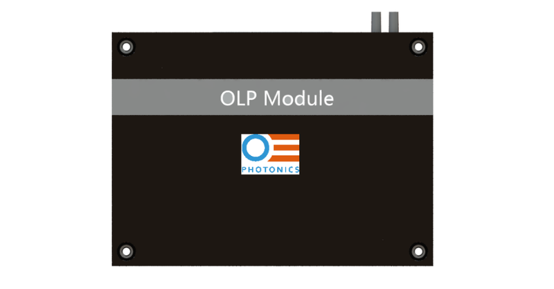 Customized OLP module
Research & Education
Oe-photonics
Wavelength Range: 1260~1650 nm Test Wavelength: 1310/1550 Switch Type: Latching/Non-Latching, 5V
OE photonics' OLP is a customer-specific module using optical switches, couplers, PDs, and related components for optical-path switching and monitoring. It is widely used in fronthaul and other optical networks.
-
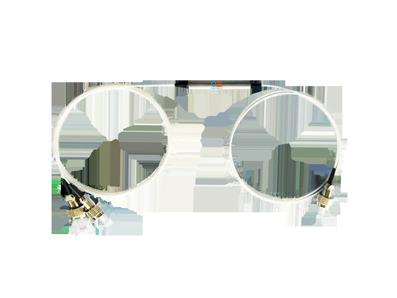 3-channel optical fiber circulator
Research & Education
Oe-photonics
Center Wavelength λc: 1310 or 1550 Wavelength Range: λc±20 Loss [λc at 23℃; IL excludes connectors]: ≤0.8 dB
OE Photonics' circulator uses the Faraday effect to transmit light in one direction while isolating reverse light. It is widely used in WDM and CATV systems.
-
 1x4/1x8 mechanical optical switch
Research & Education
Oe-photonics
Wavelength: 850±50/1310±50/1260~1650 Return Loss [MM]: ≥30 dB Return Loss [SM]: ≥50 dB
OE Photonics' mechanical 1x4 and 1x8 switches select channels between input and output light. Compact size, long life, and stable reliability suit optical-path protection, channel switching, and related optical networks.
-
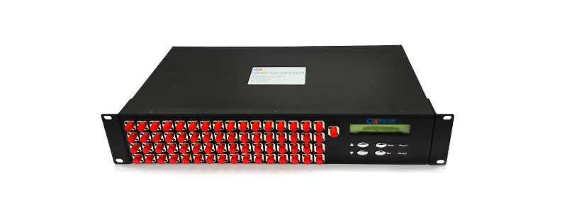 Optical switch test equipment
Research & Education
Oe-photonics
Polarization Dependent Loss PDL: ≤0.15 dB Wavelength Dependent Loss WDL [CWL±30nm,23℃]: ≤0.3 dB Temperature-Dependent Loss TDL: ≤0.3 dB
OE photonics' optical-switch tester changes channels through buttons or RS232 and is widely used in optical-communications manufacturing.
-
 Mode-conversion patch cord
Research & Education
Oe-photonics
Mode field conversion: 9um to 6.5um Mode field conversion: 9um to 4.8um Mode field conversion: 9um to 4.0um
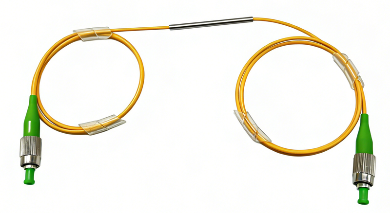
OE photonics' mode-field-conversion patch cord serves links between optical devices or between networks and devices requiring a mode-field change. After conversion and adjustment by equipment such as a power amplifier, the desired fiber mode field is obtained. It mainly converts between single-mode SM 9/125um and small mode fields of 6um, 4um, or 3um in patch-cord form. FC, SC, LC, and other connectors can be fitted to customer requirements.
Related Articles
For low-frequency RF, electromagnetic testing and power combining systems, conventional resistive power dividers bring high insertion loss, while standard directional couplers cannot provide equal-amplitude signals with 180° phase shift. They fail differential circuits, balanced amplifiers and signal cancellation systems.
Wuhan Optics Valley Quantum Technology Co., Ltd. is a leading domestic developer of high‑speed semiconductor optical chips and photodetector components. Our product portfolio covers InGaAs avalanche photodiode bare dies and PIN photodetector chips designed for fiber‑optic communication
Recently, the key laboratory of Functional Crystal Materials of Tianjin University has published a cutting-edge research paper titled Enhanced Second-Harmonic Generation in Quadratically Nonlinear Weyl Semimetal NbAs for Broadband Photodetection Applications on Advanced Science, a top-tier international academic journal.
Driven by fast‑growing demands of 3D perception, biometric authentication and machine‑vision industries, near‑infrared imaging optics have become a vital hardware component for intelligent sensing systems.
Loading...
Name
Phone
Organization
Use Case

Database Platform