

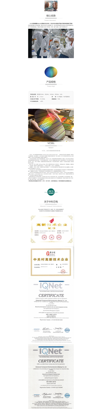
Optoelectronic gallium arsenide epitaxial wafers—Vertical-cavity surface-emitting laser (VCSEL) structure materials
Key indicators of Zhongke Xindian's VCSEL and other products reach international levels. Taking the 6-inch PHEMT as an example, Zhongke Xindian achieves levels comparable to international products in core indicators including electron mobility, two-dimensional electron gas concentration, epitaxial material nonuniformity and surface defect density.
 Save to Favorites
Overview
Specifications
| Parameter | Value |
|---|---|
| Epitaxial compound | Gallium arsenide GaAs, AlGaAs, InGaAs, AlGaAs, InAs |
| Wafer Size | 2–6 inch |
| Doping | Si (N-type dopant), Be (P-type dopant) |
| Bandwidth under the 85-degree operating condition [The original image states only Gb; /s is not added and it is not changed to GHz] | 10–25 Gb |
| Threshold Current [The original image uses uppercase MA; it has not been changed to mA] | 1 MA |
| PCE photoelectric conversion efficiency | >40 % |
Datasheet
Please provide your email to download the datasheet.
Invalid email format. Please try again.
Supplier Information
Related Products
-
100mW 1310nm CW DFB
Laser Diodes
Mindsemi
Product Rate: CW
-
1270nm DFB(10G)
Laser Diodes
Mindsemi
Product Rate: 10G
-
1270~1330nm CWDM4 DFB(10G)
Laser Diodes
Mindsemi
Product Rate: 10G
-
1270~1330nm CWDM4 DFB(25G)
Laser Diodes
Mindsemi
Product Rate: 25G
-
1270~1370nm CWDM6 DFB
Laser Diodes
Mindsemi
Product Rate: 25G
Related Articles
Founded in Beijing in 2011, Beijing FJR Opto-electronic Technology Co., Ltd. specializes in R&D, manufacturing and sales of infrared thermal imaging equipment and complete optoelectronic systems.
On November 28, 2024, the 3rd China Laser Star Enterprise Summit & Advanced Laser Processing Technology Summit, an annual influential event in the laser industry, was grandly held in Wuhan Optics Valley.
As fundamental refractive optical components, plano‑convex spherical lenses consist of one convex spherical surface and one flat surface.
As premium broadband light sources situated between traditional LEDs and laser diodes, MicroLight superluminescent‑diode (SLD) products combine broad spectral bandwidth, sufficient optical output power and low‑coherence performance.
Loading...
Name
Phone
Organization
Use Case

Database Platform