

GaAs- and InP-based avalanche photodiode (APD) epitaxial wafers
ACS develops and manufactures high-quality avalanche photodiodes using a range of advanced technologies. Materials and fabrication processes can be adjusted and customized to customer requirements, including sensitivity at different wavelengths, speeds and capacities. ACS is committed to manufacturing suitable products for you. An APD, or Avalanche Photodiode, is an optical receiver device primarily used to detect weak optical signals after transmission, amplify and reshape them, and regenerate the original transmitted signal. It is a photodetection device that converts optical signals into electrical signals through the photoelectric effect. APD operating principle: Electrons and holes generated through the photoelectric effect are rapidly accelerated in a high-electric-field region and may collide with other atoms repeatedly, causing a rapid increase in carriers and reverse current and producing avalanche multiplication. The main reason for choosing an APD is the high receiver sensitivity obtained by multiplying the photocurrent through avalanche multiplication.
 Save to Favorites
Overview
Applications
Key Features
Datasheet
Please provide your email to download the datasheet.
Invalid email format. Please try again.
Supplier Information
Related Products
-
 200um MPD photodetector
Photodiodes
Mindsemi
-
250um MPD photodetector
Photodiodes
Mindsemi
-
4×25G PD Array
Photodiodes
Mindsemi
Product Rate: 25G
-
APD
Photodiodes
Mindsemi
-
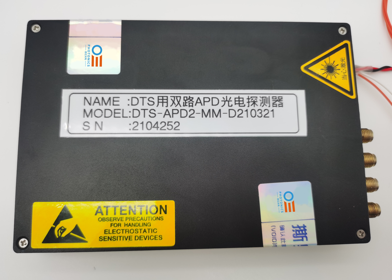 Dual-channel APD photodetector for DTS (DTS-APD2)
Photodiodes
Oe-photonics
Operating Wavelength [APD]: min:900 nm; max:1700 nm Responsivity [APD]: typical:8.5 A/W; max:20 A/W Avalanche voltage V_BR [APD]: min:40 V; max:60 V
The DTS-APD2 integrates 2 groups of single-mode/multimode WDM and APD detectors for distributed fiber temperature sensing, separately detecting Stokes and Anti-Stokes signals. Built-in constant-temperature and constant-voltage control keeps APD chips stable, with low temperature drift and noise. Multistage amplification and noise suppression improve weak-signal output quality and system signal-to-noise ratio. A single DC+5V supply powers the module. Internal precision drive and logic circuits allow parameter configuration through a serial port and host software.
Related Articles
Founded in Beijing in 2011, Beijing FJR Opto-electronic Technology Co., Ltd. specializes in R&D, manufacturing and sales of infrared thermal imaging equipment and complete optoelectronic systems.
On November 28, 2024, the 3rd China Laser Star Enterprise Summit & Advanced Laser Processing Technology Summit, an annual influential event in the laser industry, was grandly held in Wuhan Optics Valley.
As fundamental refractive optical components, plano‑convex spherical lenses consist of one convex spherical surface and one flat surface.
As premium broadband light sources situated between traditional LEDs and laser diodes, MicroLight superluminescent‑diode (SLD) products combine broad spectral bandwidth, sufficient optical output power and low‑coherence performance.
Loading...
Name
Phone
Organization
Use Case

Database Platform