
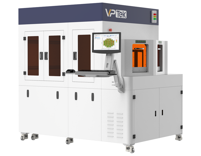
Tornado 2000 Crystal Circle Surface Deficiencies Detection Device
Tornado 2000 is a micro-precision-based crystal-round fully automated optical detection device introduced by Whip, based on advanced two-way optical imaging systems and various lighting programmes to adapt to optical imaging problems of various materials, supports testing models such as D2D, D2G, C2C, D2DB, AI, which can be applied to large-scale DIE, non-arrayd-based routing crystal-round defects, and Torando 2000 is based on flexible hardware configurations that can be applied to the detection of defects in the front, back-track processes.
 Save to Favorites
Overview
Applications
Key Features
Datasheet
Please provide your email to download the datasheet.
Invalid email format. Please try again.
Supplier Information
Related Products
-
 Post-Evaporation Inspection System
Semiconductor Manufacturing Equipment
Lic-vision
-
 Lithography System
Semiconductor Manufacturing Equipment
Trusee
-
 Resist Stripping System
Semiconductor Manufacturing Equipment
Trusee
-
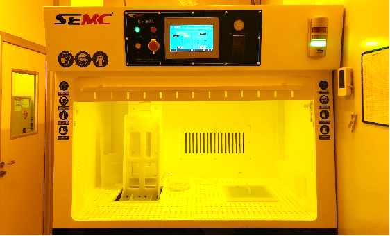 Developing System
Semiconductor Manufacturing Equipment
Trusee
-
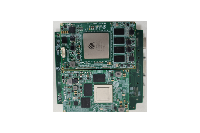 Image Recognition and Tracking Board
Semiconductor Manufacturing Equipment
Tera-aurora
Main Processor [FPGA]: Fudan Micro 7K325t Main Processor [ARM]: HiSilicon 3403 Storage [FPGA]: 32G EMMC, 64G SD Card
Image Recognition and Tracking Board
Related Articles
Laser pump sources are the core energy input component of solid-state lasers and laser amplifiers, and their performance directly determines the output power, beam quality and service life of the entire laser system. In scenarios such as industrial processing, scientific research experiments and high-end equipment, improper pump source selection will not only result in substandard system performance, but also bring a series of problems such as rapid device degradation and high operation and maintenance costs. This article sorts out the core selection logic and key pitfalls of pump source procurement, and provides selection references based on mature, mass-produced high-reliability products to help purchasers efficiently screen suitable products.
Shandong Haucore Optoelectronics Co., Ltd. introduces the HGLD‑792‑COS‑D‑10WB semiconductor laser within its COS series. Delivering an output power of 10 W at a central wavelength of 792 nm, this device adopts gold‑tin bonding COS packaging. Featuring high reliability and long service life, it serves as a preferred pump source for solid‑state lasers and is widely deployed in industrial processing, laser display, medical & aesthetic treatment, scientific research and other fields.
Fomoptic delivers integrated one‑stop optical solutions covering precision optical fabrication and custom vacuum coating services. Supported by complete processing production lines, comprehensive metrology equipment and experienced engineering team, we provide full‑chain customized components, ranging from blank shaping, ultra‑precision polishing to thin‑film coating, for laser systems, infrared imaging, industrial optics and scientific‑research projects.
Fiber lasers and fiber amplification systems require excitation sources with stable wavelength, narrow spectral linewidth and consistent output power.
Loading...
Name
Phone
Organization
Use Case

Database Platform