

Lambda Microscopic Hyperspectral Imaging Systems Lambda-Nir
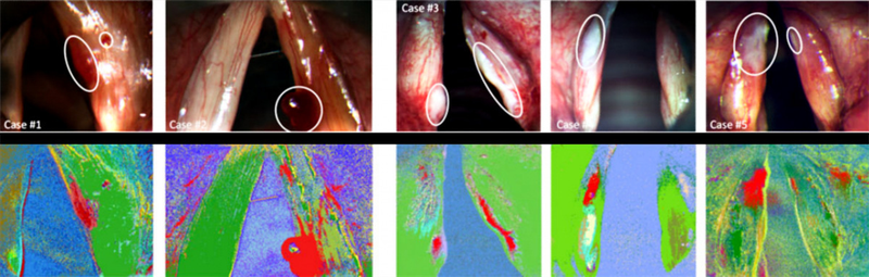
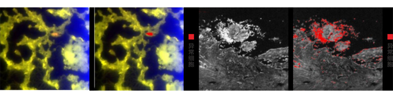
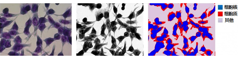
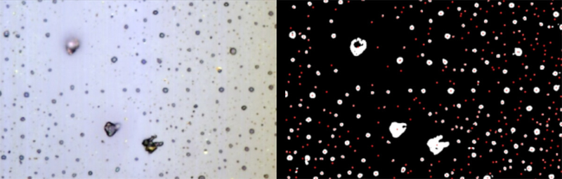
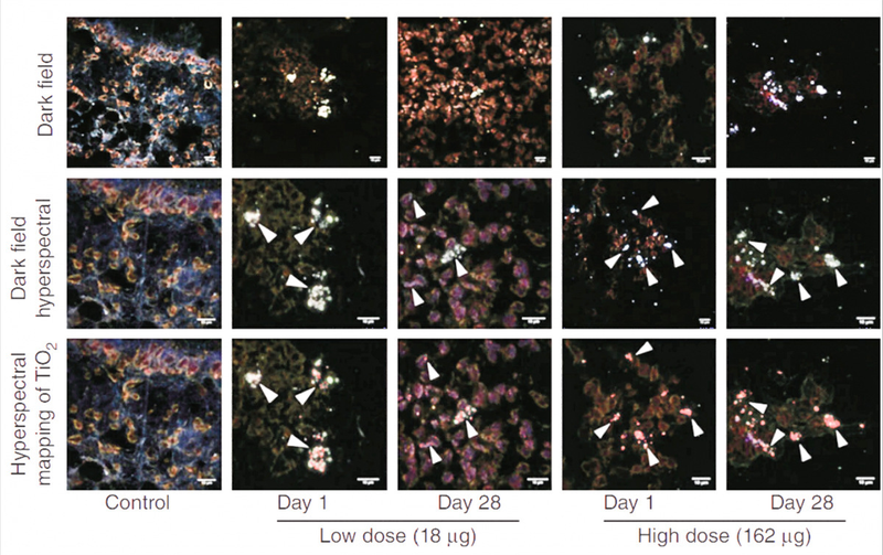
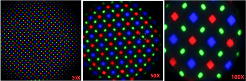
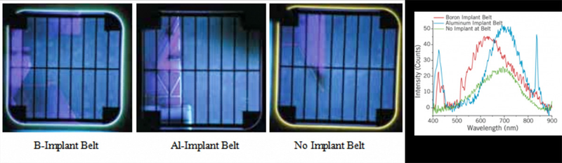
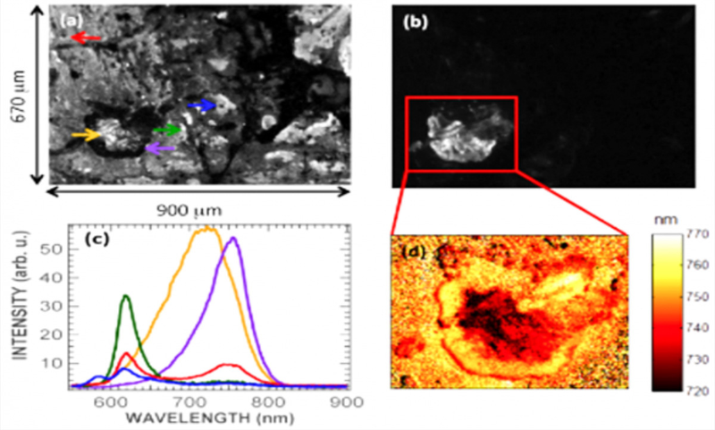
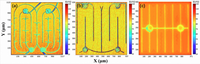
Lambda microscopic hyperspectral imaging fits most commercial microscopes. An area detector, drive supply, motion control and acquisition modules are integrated without a motorized stage, greatly reducing size/weight for simple microscope operation. Applications include tumor-cell identification, hemorrhagic-polyps/fleshy-white-patch identification, lymphocytic-leukemia screening, cytoplasm/nucleus discrimination and cell counting. Darkfield excludes unrelated light from the objective, revealing clear outlines on a dark background; particles as small as 4~200nm can be seen, with resolution stated as 50 times ordinary brightfield. Hyperspectral microscopy identifies particle types. The figure uses VNIR imaging of mouse lung after a single low (18 pg) or high (162 pg) intratracheal titanium-dioxide nanoparticle dose to locate retained particles. Darkfield hyperspectral images show white-inclusion aggregates in the middle image; hyperspectral maps show red dots/aggregates below. Different eyepiece magnifications produce high-spatial-resolution OLED emission images, combining images/spectra to inspect uniformity/stability. Noncontact, nondamaging, rapid microregion measurement operates at room temperature or inline, obtaining whole-wafer PL Mapping for substrate/epilayer composition ratios, defects and other microregional uniformity. It identifies wafer materials and changes in emission-center concentration at fine scales. Compared with confocal imaging for perovskite inhomogeneity, advantages include single full-field imaging, uniform excitation intensity across the PL field and quantitative spectral intensity. Semiconductor uses include emission uniformity, defect analysis and spatial LED-chip temperature distributions. Additional cases from readable page text: rapid hyperspectral identification of laryngeal mucosal hemorrhagic polyps/fleshy-white-patch regions, shown red; tumor/abnormal-cell spread at 20-times eyepiece magnification; rapid nucleus/cytoplasm/other-material discrimination; counting by cell centroids, total 402; darkfield nanoparticle-exposed tissue, upper image; OLED emission at 20X,50X,100X; images/spectra of boron-implanted, aluminum-implanted and special unimplanted wafers; perovskite PL data: (a)/(b) are monochromatic images at 625nm/750nm, (c) spectra from different positions in Figure 1, (d) regional PL spectral-shift imaging; hyperspectral inversion of temperatures on different LED source panels.
 Save to Favorites
Overview
Specifications
| Parameter | Value |
|---|---|
| Spectral Range | 1150~1650±5nm |
| Spectral Resolution | 20nm |
| Number of Spectral Channels | 32/64 |
| Standard Lens-Focal Length [Other optional focal lengths: 9mm, 15mm, 22mm, 56mm; inquire about other options] | 35 (other focal lengths optional) |
| Standard Lens-Working Distance | 300-∞ |
| Standard Lens-Field of View | 15.6° |
| Detector | 640×512 InGaAs FPA |
| Pixel Count (Spatial Dimension × Scan Dimension) | 640×512 |
| Pixel Size | 15 μm × 15 μm |
| Digital Output | 14bit |
| Frame Count | 10μs-1s |
| Built-in Computer Interface | USB3.0+HDMI |
| Lens Mount | C-Mount |
| System Power Supply [DC] | DC 16.8V |
| Built-in Microprocessor | I7 processor, 16G RAM, 256G SSD |
| Built-in Battery | 65Wh |
| System Power Consumption | 60W |
Applications
Key Features
Datasheet
Supplier Information
Related Products
-
Aurora 900 structured-light depth camera Scientific & Industrial Cameras Deptrum
Overall System Dimensions [Without mounting wings]: 61mm*18mm*13.5mm Baseline: 40mm Interface: USB 2.0 Wafer receptacle interface
The Deptrum® Aurora 900 is a compact, low-power, high-performance 3D structured-light depth camera. High-performance depth ASIC, ISP, and AI modules support Face AE and high-quality color, infrared, and depth images across lighting conditions. A built-in encryption chip digitally signs images to prevent tampering. The Aurora 900 has WeChat Pay and BCTC certification for WeChat and UnionPay facial payments, as well as door locks, access control, volume measurement, and other uses.
-
Aurora 910 depth camera Scientific & Industrial Cameras Deptrum
Overall System Dimensions [Without mounting wings]: 61mm*18mm*13.5mm Baseline: 40mm Interface: USB 2.0 Wafer receptacle interface
Based on speckle structured light, an in-house 3D structured-light depth soft-core reconstruction algorithm captures three-dimensional object and spatial structures. Fusing camera RGB images with depth data provides convenient, efficient 3D perception. Depth HDR and closed-loop RGB/IR Face AE provide high-quality facial images at 100000Lux. Deptrum's BCTC enhanced-level facial-liveness solution provides a complete offering for facial payment, access control, and subway passage.
-
Aurora 930 depth camera Scientific & Industrial Cameras Deptrum
Overall System Dimensions [Without mounting wings]: 61mm*18mm*14.3mm Baseline: 40mm Interface: USB 2.0 Wafer receptacle interface
The Deptrum® Aurora 930 depth camera uses 3D structured light to capture object and spatial structures. High-performance ISP and ASIC depth-processing chips output high-quality color, infrared, and depth images over 3-80,000Lux, maintaining quality under low light, backlighting, and other difficult conditions. Applications include robot obstacle avoidance and volume measurement.
-
HandPass 100 dual-modality camera Scientific & Industrial Cameras Deptrum
Complete-unit diameter: 85.39mm Complete-unit thickness: 19.9mm Baseline: 14mm
The Deptrum® HandPass 100 dual-modal palm-recognition camera combines precision optics, high-performance ISP and AI modules, and a soft-core AE algorithm for fast palm detection and self-closed-loop Palm AE. It provides high-quality palmprint and palm-vein images in low light, backlighting, and other conditions. A built-in encryption chip signs images to prevent tampering and protect payment data. Applications include palm-recognition access control, subway gates, smart buildings, and offline payment.
-
Libra 1000 depth camera Scientific & Industrial Cameras Deptrum
Module dimensions: 38.9 mm × 42 mm × 22.24 mm Baseline: 2cm Interface: GMSL 2.0 Fakra interface
The Libra 1000 depth-camera series uses binocular 3D imaging to capture object and spatial structures. A high-performance ISP and image-processing engine output preprocessed binocular images. Combined with a high-performance depth-reconstruction SDK, it enables robots to reconstruct binocular depth with ultrahigh precision at close range.
Related Articles
The LZFL405‑80mW‑3 series from Shenzhen Leirte Optoelectronics Co., Ltd. is a coaxial‑packaged violet‑blue single‑mode fiber‑coupled laser diode. It delivers 80 mW continuous‑wave output at 405 nm. Light is coupled into 3 μm core‑diameter single‑mode fiber for clean beam quality and easy integration into diverse optical systems. It serves as a compact violet‑blue light source for medical instruments and industrial printing applications.
Wuhan Optics Valley Quantum Technology Co., Ltd. is a leading domestic developer of high‑speed semiconductor optical chips and photodetector components. Our product portfolio covers InGaAs avalanche photodiode bare dies and PIN photodetector chips designed for fiber‑optic communication
As a professional ultraviolet‑laser solution provider, Precilasers has launched its 266 nm narrow‑linewidth industrial laser, delivering reliable single‑frequency output for high‑precision interference lithography, semiconductor inspection and precision metrology applications.
Electro-optic deflectors (EODs) are optical devices used to steer or deflect light beams by applying an electric field to a specialized optical crystal. Unlike mechanical beam steering systems that rely on moving mirrors, electro-optic deflectors enable high-speed, non-mechanical beam control with exceptional precision and responsiveness. They are widely used in laser scanning, optical communications, microscopy, laser printing, spectroscopy, and scientific research, where rapid and accurate laser beam positioning is essential.
Loading...
Name
Phone
Organization
Use Case

Database Platform