

QC Series Compact Low-Power RF Driver QCXXX-YYDC-ZZZ-AAV
The QC series is a compact low-power RF driver for AOMs and acousto-optic Q-switches, covering24–110 MHz with up to24 W into50 Ω. Digital modulation, analog power control, zero-crossing synchronization, and configurable output power meet industrial, research, and OEM needs. Contact conduction cooling, compact construction, configurable modes, and integrated modulation provide reliability, heat dissipation, and easy integration in space-limited lasers and optoelectronics. Two TTL digital inputs support fixed-width pulses set internally or variable-width pulses controlled externally. Analog input continuously adjusts RF power. Factory-configurable modes include analog power control, switched analog control, first-pulse suppression, and prepulse elimination to improve laser output and control. Zero-crossing synchronization aligns RF pulses with RF zero crossings to reduce pulse jitter and improve repeatability and stability in timing-sensitive lasers. QC drives Q-switches for stable pulsed-laser generation and AOMs for pulse picking, high-speed intensity modulation, and precision control in industrial and ultrafast lasers, precision processing, research, and optoelectronics. Applicable devices:acousto-optic modulators and air-cooled Q-switches. ¹Voltage range corresponds to0%–100% of preset maximum RF power and applies to acousto-optic devices configured with A05,R05,and M05. ²Into50 Ω. ³ZC enables zero-crossing by default. Status LEDs:Red |Normal Operation;Green |Standby;Yellow |Fault. Mating plug:Molex0430251200 with Molex0430300008 crimp terminals. Heat-sink capacity required:36 W@12 V,45 W@15 V,72 W@24 V. Power/control connector:12 pins,3.00 mm (0.118") pitch. Unless stated otherwise, inputs reference GND; outputs are open-collector with maximum sink current25 mA. Pin1 |SYNC Output;Pin2 |FPS Trigger Input;Pin3 |Fixed-Width Modulation Input;Pin4 |GND;Pin5 |Variable-Width Modulation Input;Pin6 |Analog Modulation Input;Pin7 |Zero-Crossing Synchronization Enable;Pin8 |Low-Power Fault Output;Pin9 |High-Power Fault Output;Pin10 |High-VSWR Fault Output;Pin11 |Enable Input;Pin12 |VDC Supply Input. Absolute Maximum Ratings Note:exceeding limits may cause instantaneous, irreversible damage; DC feedback at the RF output is prohibited. Adjustments:RF Power Level |Clockwise increases output power. Low-Power Threshold |Below the minimum threshold, LP Fault goes low.* High-Power Threshold |Above the maximum threshold, HP Fault goes low. High-VSWR Protection Threshold |Sets load-mismatch tolerance; mismatch drives the fault low, turns the LED yellow, and stops output; enter standby and resume to reset. Fixed Pulse Width |Adjusts RF-off duration over1~20 μs. FPS/PPK-Only Adjustments:FPS Initial Power |Sets first-pulse output;FPS Slope |Sets recovery to normal RF power after FPS starts,20~300 μs;FPS Window |Sets suppression duration,20~300 μs. *Analog RF-power modulation automatically masks LP Fault. Ordering:XXX =024,027,041,068,080,or110 as standard, corresponding to RF frequencies24.00,27.12,40.68,68.00,80.00,or110.00 MHz.
 Save to Favorites
Overview
Specifications
| Parameter | Value |
|---|---|
| Power Supply Voltage [Factory-set] | +12 VDC、+15 VDC or +24 VDC( Factory-set ) |
| Power Supply Current | ≤3 A |
| RF Output Power [50 Ω Load] | 2~24 W |
| Output Impedance | 50 Ω |
| RF Frequency | 24.00 MHz、27.12 MHz、40.68 MHz、68.00 MHz、80.00 MHz or 110.00 MHz |
| Frequency Stability | ±0.01% |
| Extinction Ratio | ≥50 dB |
| Harmonic Distortion [RF Output Power≤15 W] | ≤-20 dBc |
| Harmonic Distortion [RF Output Power>15 W] | ≤-15 dBc |
| Spurious Level | ≤-50 dBc |
| Analog Modulation Input Impedance | 1.5 kΩ |
| Analog-Modulation Input Voltage [0%–100% of Preset Maximum RF Power;A05,R05 and M05 Configurations;Footnote¹] | 0~+5 VDC¹ |
| Digital Modulation Input Impedance | High Impedance |
| Digital Modulation Input Level | TTL Compatible (V_IL < 0.8V,V_IH > 2.0 V) |
| Fixed-Width Modulation | Standard:Rising-Edge Trigger;NEG Inverting-Input Option:Falling-Edge Trigger |
| Variable-Width Modulation | Standard:TTL High (TTL V_IH) Disables RF Output;NEG Inverting-Input Option:TTL Low (TTL V_IL) Disables RF Output |
| FPS / PPK Input Impedance | High Impedance |
| FPS/PPK Input Level | TTL Compatible (V_IL < 0.8V,V_IH > 2.0 V) |
| FPS/PPK Trigger Mode | Standard:Rising-Edge Trigger;NEG Option:Falling-Edge Trigger |
| Zero-Crossing Synchronization Enable Input Impedance | High Impedance |
| Zero-Crossing Synchronization Enable Input Level | TTL Compatible (V_IL < 0.8V,V_IH > 2.0 V) |
| Operating Method | Standard Version:TTL High or Floating Disables Zero-Crossing Synchronization;TTL Low Enables It |
| Sync Out | Output Level:3.3 V;ZC Version Output Is Inverted |
| Enable Control - Normal Operation | TTL High or Floating |
| Enable Control - Standby | TTL Low (Standby Consumption<3 W) |
| Enable Control - Driver Reset | Momentary TTL Low |
| Rise/Fall Time [Number / Analog Modulation ;10%–90% RF Output Power ;50 Ω Load ( Footnote ²)] | ≤35 ns( Number / Analog Modulation ,10%~90% RF Output Power )² |
| Operating Temperature [Case Temperature;Noncondensing] | +10 ℃~+55 ℃ (case temperature, non-condensing) |
| Storage Temperature [non-condensing] | -20 ℃~+85 ℃( non-condensing ) |
| Operating Method [ZC Option;Zero-Crossing Enabled by Default (Footnote³)] | TTL High or Floating Enables Zero-Crossing Synchronization;TTL Low Disables It |
| RF Output Connector | MA Female (Recommended Tightening Torque0.45 N·m, Maximum0.6 N·m) |
| Power Supply / Control Interface | Molex 0430451221 |
| Cooling Method | Contact Conduction Cooling |
| Weight [Driver Only] | 192 g (Driver Only) |
| Maximum Supply Voltage [Absolute Maximum Ratings] | +27 VDC |
| TTL/Analog Input [Absolute Maximum Ratings] | -0.5 V~+5.5 V |
| Minimum Pulse Width in Fixed-Width Mode [Absolute Maximum Ratings] | 50 ns |
| Modulation Repetition Rate [Absolute Maximum Ratings;Fixed-Width Modulation;Source Range Endpoints Use Different Units] | 1 Hz~1 MHz |
| Modulation Repetition Rate [Absolute Maximum Ratings;Variable-Width Modulation] | DC~10 MHz |
| Maximum Output Power [Supply Voltage :12 V; RF Frequency :24 MHz] | 10 W |
| Maximum Output Power [Supply Voltage :12 V; RF Frequency :27.12 MHz] | 10 W |
| Maximum Output Power [Supply Voltage :12 V; RF Frequency :40.68 MHz] | 10 W |
| Maximum Output Power [Supply Voltage :12 V; RF Frequency :68 MHz] | 10 W |
| Maximum Output Power [Supply Voltage :12 V; RF Frequency :80 MHz] | 10 W |
| Maximum Output Power [Supply Voltage :12 V; RF Frequency :110 MHz] | 10 W |
| Maximum Output Power [Supply Voltage :15 V; RF Frequency :24 MHz] | 24 W |
| Maximum Output Power [Supply Voltage :15 V; RF Frequency :27.12 MHz] | 24 W |
| Maximum Output Power [Supply Voltage :15 V; RF Frequency :40.68 MHz] | 24 W |
| Maximum Output Power [Supply Voltage :15 V; RF Frequency :68 MHz] | 20 W |
| Maximum Output Power [Supply Voltage :15 V; RF Frequency :80 MHz] | 20 W |
| Maximum Output Power [Supply Voltage :15 V; RF Frequency :110 MHz] | 10 W |
| Maximum Output Power [Supply Voltage :24 V; RF Frequency :24 MHz] | 24 W |
| Maximum Output Power [Supply Voltage :24 V; RF Frequency :27.12 MHz] | 24 W |
| Maximum Output Power [Supply Voltage :24 V; RF Frequency :40.68 MHz] | 24 W |
| Maximum Output Power [Supply Voltage :24 V; RF Frequency :68 MHz] | 24 W |
| Maximum Output Power [Supply Voltage :24 V; RF Frequency :80 MHz] | 24 W |
| Maximum Output Power [Supply Voltage :24 V; RF Frequency :110 MHz] | 10 W |
| Fixed Pulse-Width Adjustment [Fixed-Width Mode;RF-Off Duration] | 1~20 μs |
| FPS Slope [FPS/PPK Models;Rate of RF Output Recovery to Normal Power after FPS Starts] | 20~300 μs |
| FPS Window [FPS/PPK Models;First-Pulse Suppression Duration Window] | 20~300 μs |
Key Features
Datasheet
Supplier Information
Related Products
-
 1CH×25G/28G DML Driver
Software and Data Services
Xy-technology
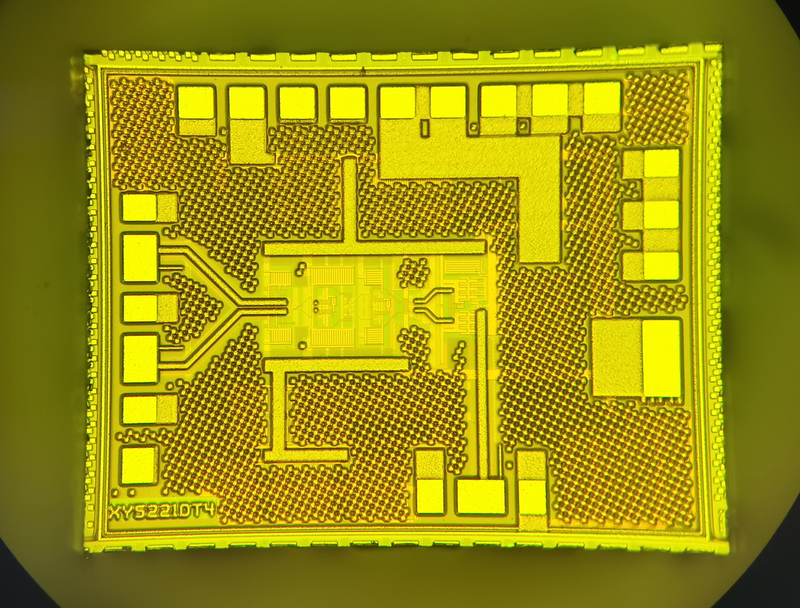
XY5221DD is One. Single Channel Laser Driver , Designed for direct modems 25Gb/s Laser Interface 。 The currents and the transients can be replaced by the currents. 2 Line Line Lines Interface Independent Programming , Meanwhile... 2 Line Interface Supports also the inclusion of programmability for balancing and cross-point adjustments , Take one. Tx Disable , It can be closed. Laser Erosion and Moderation Current , Existing IBIAS Monitor 。 This simulation output can be used to Laser Overcrowding and / or Laser Modulation Current for External Monitoring 。 There's a piece in there. ADC Functions , It can be used for foot-inducing measurements via electrical input of a special back-cover monitor TX_PWR。ADC It can also be configured for measurement. VCC( ..can measure each Power Supply ) and IBIAS( Average Laser Erosion of currents )。
-
 1CH×25G/28G EML Driver
Software and Data Services
Xy-technology
XY5221E is A high-performance piece. Single Channel 28Gbps EML Driver 。 It provides daring. 30GHz High bandwidth and greater than 2.5Vpp and the output range , The cost of the operation is about 0.17W。 It's designed for use in... Drive EML Laser , The chip is available in nudity chip form. 。
-
 4CH×25G/28G DML Driver
Software and Data Services
Xy-technology
XY5224DD is One. Four Channel Laser Driver , Designed for direct modems 25Gb/s Laser Interface 。 The currents and the transients can be replaced by the currents. 2 Line Line Lines Interface Independent Programming , Meanwhile... 2 Line Interface Supports also the inclusion of programmability for balancing and cross-point adjustments , Take one. Tx Disable , It can be closed. Laser Erosion and Moderation Current , Existing IBIAS Monitor 。 This simulation output can be used to Laser Overcrowding and / or Laser Modulation Current for External Monitoring 。 There's a piece in there. ADC Functions , It can be used for foot-inducing measurements via electrical input of a special back-cover monitor TX_PWR。ADC It can also be configured for measurement. VCC( ..can measure each Power Supply ) and IBIAS( Average Laser Erosion of currents )。
-
4CH×25G/28G EML Driver
Software and Data Services
Xy-technology
XY5224E is A high-performance piece. Four Channel 28Gbps EML Driver 。 It provides daring. 30GHz High bandwidth and greater than 2.5Vpp and the output range , The cost of the operation is about 0.45W。 It's designed for use in... Drive EML Laser , The chip is available in nudity chip form. 。
-
 25G/28G CDR+VCSEL Driver
Software and Data Services
Xy-technology
XY5921V Integration VCSEL Driver 、 Balancer and clock data recovery 。 None The reference clock will support it. 24.3Gbps Present. 28.1Gbps Rate range , It's also possible. bypass Mode supports lower rate 。 The chip is provided in nudist form. 。
Related Articles
Driven by the continuous pursuit of higher precision and efficiency in optical communication and optoelectronic device manufacturing, OLCR-1000 Low-Coherence Interferometer, independently developed by Wuhan Guanggu Interconnect Technology Co., Ltd., provides an innovative technical solution for distributed return loss testing of optical fibers and optoelectronic devices.
icrolight is a high-tech enterprise specializing in the R&D, manufacturing and sales of active and passive photonic devices for microwave photonics, LiDAR ranging, gas sensing, fiber optics and photomedicine.
BEIJING JIEPU TREND supplies YAG+Er:YAG+YAG bonded composite slab laser crystals for high‑power solid‑state laser systems. The monolithic slab consists of two undoped YAG end‑cap layers and a central Er‑doped YAG gain segment. The overall dimension is 9 mm×9 mm×9 mm.
Shanghai Connet Laser Technology Co., Ltd. focuses on technological innovation, delivering cutting-edge photonic products & solutions for industrial lasers, LiDAR, fiber optic sensing, coherent telecom, cold atom physics and precision spectroscopy research & mass manufacturing.
Loading...
Name
Phone
Organization
Use Case

Database Platform